UG-868 ADuCM320i/ADuCM322/ADuCM322i Reference Manual
Rev. B | Page 20 of 192
ADC CIRCUIT OVERVIEW
The ADuCM320i/ADuCM322/ADuCM322i incorporates a fast, multichannel, 16-bit ADC. The ADC is specified to be 14-bit (ADuCM320i)
or 12-bit (ADuCM322/ADuCM322i) accurate. It can operate from a 2.9 V to 3.6 V supply and is capable of providing a throughput of up
to 1 MSPS. This ADC block provides the user with a multichannel multiplexer, input buffer for high impedance input channels (ADuCM320i
only), on-chip reference, and SAR ADC.
The SAR ADC circuit is implemented on the low voltage analog die. The ARM Cortex-M3 processor interfaces to the ADC via an
internal parallel die to die interface.
Depending on the input signal configuration, the ADC can operate in one of the following two modes:
Differential mode measures the difference between two signals.
Single-ended mode measures any signal relative to AGND.
The converter accepts an analog input range of 0 to V
REF
when operating in single-ended mode. In fully differential mode, the input signal
must be balanced around a common-mode voltage (V
CM
) in the 0 V to AV
DD
range and with a maximum amplitude of 2 × V
REF
.
0
AV
DD
FS (V
REF
)
–FS (–V
REF
)
IN+
AIN–
OUTPUT CODE
13437-105
Figure 6. Examples of Balanced Signals for Differential Mode
A high precision, low drift, factory-calibrated 2.51 V reference is provided on-chip. An external reference can also be connected to the
ADC_REFP and ADC_REFN pins.
Single or continuous conversion modes can be initiated in the software. An external pin (alternate function of P2.4) can also generate a
repetitive trigger for ADC conversions.
ADC CIRCUIT OPERATION
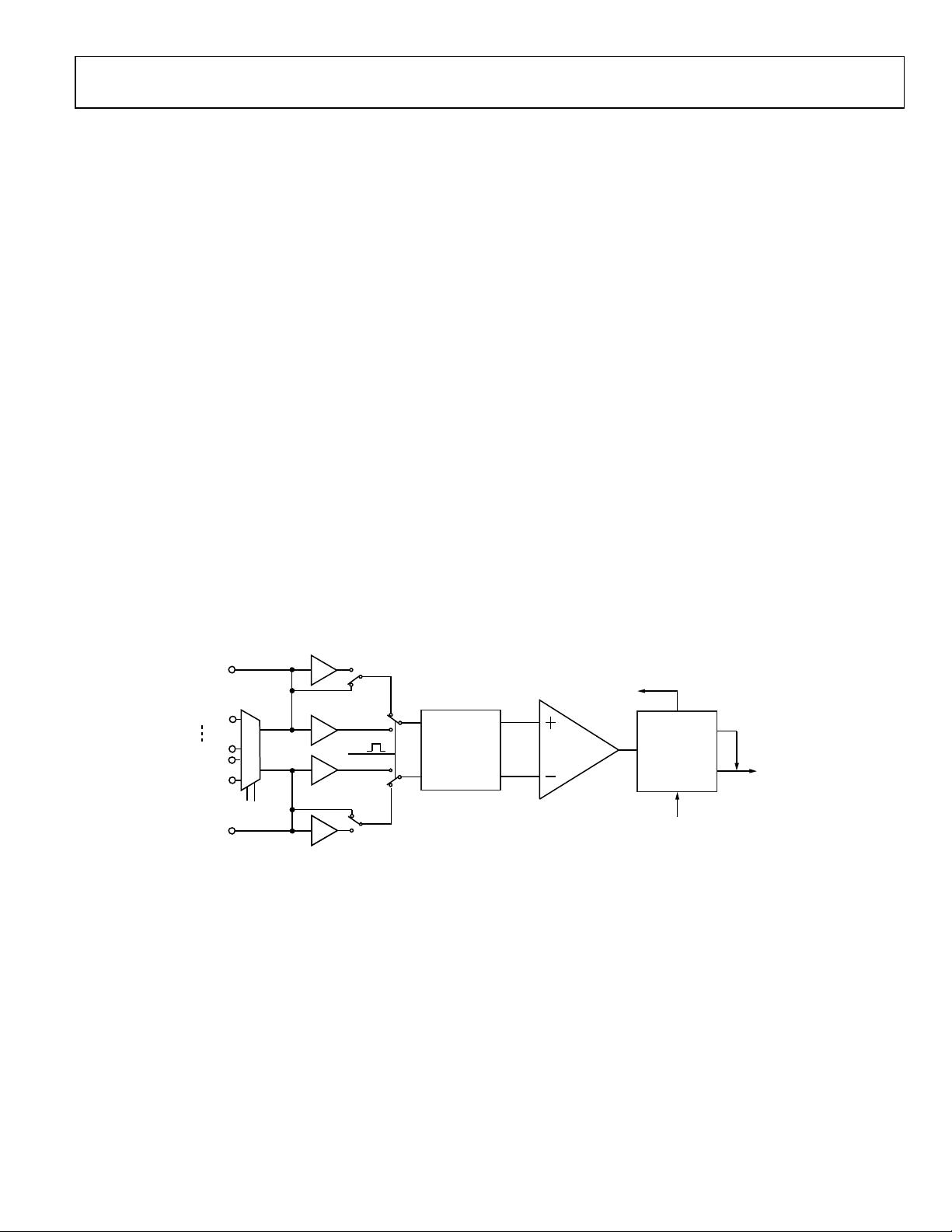
The SAR ADC is based on a charge redistribution DAC. The capacitive DAC consists of two identical arrays of 18 binary weighted
capacitors that are connected to the two inputs of the comparator.
The ADC converts the voltage applied to AIN+ and AIN− in the following three phases:
1. During the precharge phase, the precharge buffers connect the inputs to the capacitor arrays, which charges the capacitors quickly
with minimal loading of the external input source.
2. During the acquisition phase, the capacitor arrays are connected directly to the inputs to fully charge the capacitor arrays and
eliminate any precharge buffer errors. The timing for the acquisition phase is set by ADCCNVC[25:16]. This value must be set to 500 ns. If
the input buffer is not used when measuring AV
DD
/2, IOV
DD
/2, or temperature sensor channels, set this value to 1.5 μs.
3. At the end of the acquisition phase, the internal CNV signal goes high and initiates the conversion phase. The conversion begins with
the SW+ and SW− switches opening, which disconnects the two capacitor arrays from the analog inputs and connects the analog
inputs to the AGND (−V
REF
) input. The conversion is completed by normal successive approximation.
The ADC block operates from an internally generated 20 MHz clock.
The ADC conversion rate is set by ADCCNVC[9:0].


