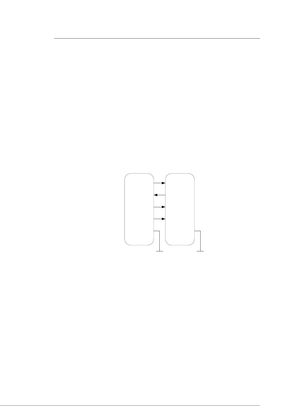
(数据输出),SCLK(时钟),CS(片选)。
(1)SDO – 主设备数据输出,从设备数据输入
(2)SDI – 主设备数据输入,从设备数据输出
(3)SCLK – 时钟信号,由主设备产生
(4)CS – 从设备使能信号,由主设备控制
其中 CS 是控制芯片是否工作,也就是说只有片选信号为预先规定的使能信号
时(高电位或低电位),对此芯片的操作才有效,否则会被忽略。这就允许在同一
主机上连接多个 SPI 设备。
其余的 3 根线是负责通信的。通讯是通过数据交换完成的,SPI 是串行通讯协
议,也就是说数据是一位一位的传输的。这就是 SCLK 时钟线存在的原因,由 SCLK
提供时钟脉冲,SDI、SDO 则基于此脉冲完成数据传输。数据输出通过 SDO 线,
数据在时钟下降沿时改变,在紧接着的上升沿被读取。完成一位数据传输,输入
也使用同样原理。这样,在至少 8 次时钟信号的改变(上沿和下沿为一次),就可
以完成 8 位数据的传输。
要注意的是,SCLK 信号线只由主设备控制,从设备不能控制信号线。同样,
在一个基于 SPI 的设备中,至少有一个主控设备。这样的传输方式有一个优点:
与普通的串行通讯不同,普通的串行通讯一次连续传送至少 8 位数据,而 SPI 允
许数据一位一位的传送,甚至允许暂停,因为 SCLK 时钟线由主控设备控制,当
没有时钟跳变时从设备不采集或传送数据。也就是说主设备通过对 SCLK 时钟线
的控制可以完成对通讯的控制。SPI 还是一个数据交换协议:因为 SPI 的数据输入
和输出线独立,所以允许同时完成数据的输入和输出。不同的 SPI 设备的实现方
式不尽相同,主要是数据改变和采集的时间不同,在时钟信号上沿或下沿采集有
不同定义。应该注意的是 SPI 主模块和与之通信的外设备时钟相位和极性应该
一致。这句话有 2 层意思:其一,主设备 SPI 时钟和极性的配置应该由外设
来决定;其二,二者的配置应该保持一致,即主设备的 SDO 同从设备的 SDO
配置一致,主设备的 SDI 同从设备的 SDI 配置一致。因为主从设备是在 SCLK
的控制下同时发送和接收数据,并通过 2 个双向移位寄存器来交换数据在点
对点的通信中。SPI 接口不需要进行寻址操作且为全双工通信,显得简单高效。在
多个从设备的系统中,每个从设备需要独立的使能信号,硬件上比 I2C 系统要稍
微复杂一些。