
ADS8364
5
SBAS219B
www.ti.com
48
47
46
45
44
43
42
41
40
39
38
37
36
35
34
33
D0
D1
D2
D3
D4
D5
D6
D7
D8
D9
D10
D11
D12
D13
D14
D15
1
2
3
4
5
6
7
8
9
10
11
12
13
14
15
16
CH A1–
CH A1+
AV
DD
AGND
SGND
CH B0+
CH B0–
AV
DD
AGND
SGND
CH B1–
CH B1+
AV
DD
AGND
SGND
CH C0+
CH A0–
CH A0+
REF
IN
REF
OUT
AGND
AV
DD
HOLD C
HOLD B
HOLD A
A0
A1
A2
ADD
RESET
BV
DD
BGND
CH C0–
CH C1–
CH C1+
NC
DGND
DV
DD
BYTE
BV
DD
BGND
FD
EOC
CLK
RD
WR
CS
BGND
64 63 62 61 60 59 58 57 56 55 54
17 18 19 20 21 22 23 24 25 26 27
53 52 51 50 49
28 29 30 31 32
ADS8364
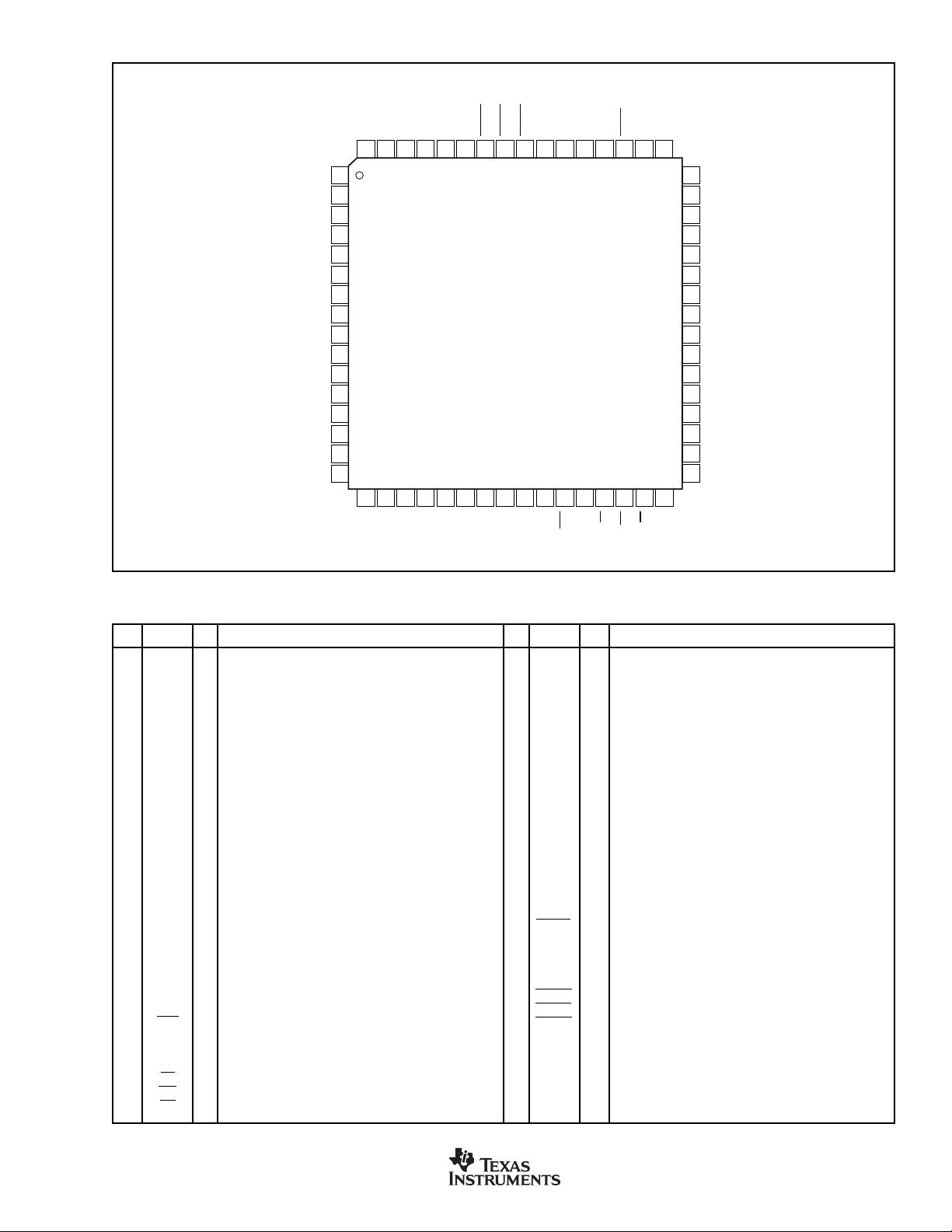
PIN CONFIGURATION
1 CH A1– AI Inverting Input Channel A1
2 CH A1+ AI Noninverting Input channel A1
3AV
DD
P Analog Power Supply
4 AGND P Analog Ground
5 SGND P Signal Ground
6 CH B0+ AI Noninverting Input Channel B0
7 CH B0– AI Inverting Input Channel B0
8AV
DD
P Analog Power Supply
9 AGND P Analog Ground
10 SGND P Signal Ground
11 CH B1– AI Inverting Input Channel B1
12 CH B1+ AI Noninverting Input Channel B1
13 AV
DD
P Analog Power Supply
14 AGND P Analog Ground
15 SGND P Signal Ground
16 CH C0+ AI Noninverting Input Channel C0
17 CH C0– AI Inverting Input Channel C0
18 CH C1– AI Inverting Input Channel C1
19 CH C1+ AI Noninverting Input Channel C1
20 NC – No Connection
21 DGND P Digital ground connected to AGND.
22 DV
DD
P +5V Power Supply for Digital Logic Connected to AV
DD
.
23 BYTE DI 2 x 8 Output Capability. Active HIGH.
24 BV
DD
P Power supply for digital interface from 3V to 5V.
25 BGND P Buffer Digital Ground
26 FD DO First Data, A0 Data
27 EOC DO End of Conversion, Active LOW
28 CLK DI An external CMOS compatible clock can be applied to
the CLK input to synchronize the conversion process to
an external source.
29 RD DI Read, Active LOW
30 WR DI Write, Active LOW
31 CS DI Chip Select, Active LOW
32 BGND P Buffer Digital Ground
33 DB15 DO Data Bit 15-MSB
34 DB14 DO Data Bit 14
35 DB13 DO Data Bit 13
36 DB12 DO Data Bit 12
37 DB11 DO Data Bit 11
38 DB10 DO Data Bit 10
39 DB9 DO Data Bit 9
40 DB8 DO Data Bit 8
41 DB7 DIO Data Bit 7, Software Input 7
42 DB6 DIO Data Bit 6, Software Input 6
43 DB5 DIO Data Bit 5, Software Input 5
44 DB4 DIO Data Bit 4, Software Input 4
45 DB3 DIO Data Bit 3, Software Input 3
46 DB2 DIO Data Bit 2, Software Input 2
47 DB1 DIO Data Bit 1, Software Input 1
48 DB0 DIO Data Bit 0, Software Input 0
49 BGND P Buffer Digital Ground
50 BV
DD
P Power Supply for Digital Interface from 3V to 5V
51 RESET DI Global Reset, Active LOW
52 ADD DI Address Mode Select
53 A2 DI Address Line 3
54 A1 DI Address Line 2
55 A0 DI Address Line 1
56 HOLDA DI Hold Command A
57 HOLDB DI Hold Command B
58 HOLDC DI Hold Command C
59 AV
DD
P Analog Power Supply
60 AGND P Analog Ground
61 REF
OUT
AO Reference Output, attach 0.1µF and 10µF capacitors.
62 REF
IN
AI Reference Input
63 CH A0+ AI Noninverting Input Channel A0
64 CH A0– AI Inverting Input Channel A0
PIN NAME I/O DESCRIPTION PIN NAME I/O DESCRIPTION
PIN DESCRIPTIONS
NOTE: AI is Analog Input, AO is Analog Output, DI is Digital Input, DO is Digital Output, DIO is Digital Input/Output, P is Power Supply Connection.
剩余21页未读,继续阅读

fengjkl
- 粉丝: 0
- 资源: 1
 我的内容管理
展开
我的内容管理
展开


最新资源
- 十种常见电感线圈电感量计算公式详解
- 军用车辆:CAN总线的集成与优势
- CAN总线在汽车智能换档系统中的作用与实现
- CAN总线数据超载问题及解决策略
- 汽车车身系统CAN总线设计与应用
- SAP企业需求深度剖析:财务会计与供应链的关键流程与改进策略
- CAN总线在发动机电控系统中的通信设计实践
- Spring与iBATIS整合:快速开发与比较分析
- CAN总线驱动的整车管理系统硬件设计详解
- CAN总线通讯智能节点设计与实现
- DSP实现电动汽车CAN总线通讯技术
- CAN协议网关设计:自动位速率检测与互连
- Xcode免证书调试iPad程序开发指南
- 分布式数据库查询优化算法探讨
- Win7安装VC++6.0完全指南:解决兼容性与Office冲突
- MFC实现学生信息管理系统:登录与数据库操作
资源上传下载、课程学习等过程中有任何疑问或建议,欢迎提出宝贵意见哦~我们会及时处理!
点击此处反馈


