1
2
3
4
5
10
9
8
7
6
REF
AVDD
AINP
AINN
GND
CONVST
DOUT
SCLK
DIN
DVDD
Thermal
PAD
1
2
3
4
5
10
9
8
7
6
REF
AVDD
AINP
AINN
GND
CONVST
DOUT
SCLK
DIN
DVDD
ADS8866
www.ti.com.cn
ZHCSBH3A –MAY 2013–REVISED DECEMBER 2013
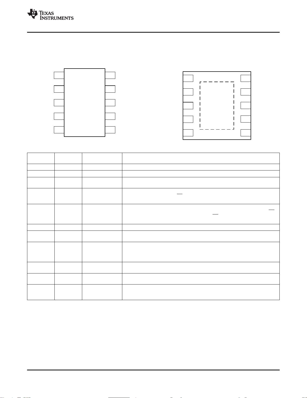
PIN CONFIGURATIONS
DGS PACKAGE
DRC PACKAGE
VSSOP-10
SON-10
(TOP VIEW, Not to Scale)
(TOP VIEW, Not to Scale)
PIN ASSIGNMENTS
PIN
PIN NAME NUMBER FUNCTION DESCRIPTION
AINN 4 Analog input Inverting analog signal input
AINP 3 Analog input Noninverting analog signal input
Analog power supply.
AVDD 2 Analog
This pin must be decoupled to GND with a 1-μF capacitor.
Convert input.
CONVST 6 Digital input This pin also functions as the CS input in 3-wire interface mode. Refer to the
Description and Timing Characteristics sections for more details.
Serial data input.
The DIN level at the start of a conversion selects the mode of operation (such as CS
DIN 9 Digital input
or daisy-chain mode). This pin also serves as the CS input in 4-wire interface mode.
Refer to the Description and Timing Characteristics sections for more details.
DOUT 7 Digital output Serial data output
Digital interface power supply.
DVDD 10 Power supply
This pin must be decoupled to GND with a 1-μF capacitor.
Device ground.
Note that this pin is a common ground pin for both the analog power supply (AVDD)
GND 5 Analog, digital
and digital I/O supply (DVDD). The reference return line is also internally connected to
this pin.
Positive reference input.
REF 1 Analog
This pin must be decoupled with a 10-μF or larger capacitor.
Clock input for serial interface.
SCLK 8 Digital input
Data output (on DOUT) are synchronized with this clock.
Exposed thermal pad.
Thermal pad — Thermal pad Texas Instruments recommends connecting the thermal pad to the printed circuit
board (PCB) ground.
Copyright © 2013, Texas Instruments Incorporated 9


 我的内容管理
收起
我的内容管理
收起
 我的收益 登录查看自己的收益
 我的积分
登录查看自己的积分
我的积分
登录查看自己的积分
 我的C币
登录后查看C币余额
我的C币
登录后查看C币余额
 我的收藏
我的收藏  我的下载
我的下载  下载帮助
下载帮助 


