二维层状材料的透射电子显微镜原位表征与操纵
34 浏览量
更新于2024-07-15
收藏 2.08MB PDF 举报
"这篇研究论文深入探讨了二维层状材料,特别是那些超越石墨烯的新型超薄材料在电子显微镜下的原位表征与操纵。这些二维材料因其丰富的物理性质和独特的层状结构,展现出巨大的潜力,在电子、化学、能源以及生物科学等领域有广泛应用。了解2D层状材料的结构、化学组成与其物理性质之间的相互作用机制对于基础纳米科学研究和下一代纳米器件的实际制造至关重要。
透射电子显微镜(TEM)凭借其高空间分辨率和多样化的外部场应用,成为原子尺度上对纳米材料和纳米器件进行静态表征和动态操纵的强大工具。近年来,薄膜技术和精密微电子机械系统(MEMS)技术的进步使得二维层状材料和纳米器件能够在TEM环境下进行更精细的研究和操作。
论文详细介绍了TEM技术如何用于揭示这些材料的结构细节,包括晶格结构、缺陷分布以及界面特性,并讨论了如何通过TEM实现对材料的精确操纵,如层间堆叠顺序的改变、缺陷修复或功能化。此外,文章还可能涵盖了在外部电场、磁场或温度变化下,2D材料的动态响应和性能调控。
通过对这些二维材料的原位观察,科学家能够实时监测材料在各种环境条件下的行为,从而对材料的稳定性、机械柔韧性和电子传输特性等关键属性有更深入的理解。这种理解对于优化材料性能、设计新的纳米器件架构以及开发新的功能化应用具有重要意义。
这篇论文全面概述了TEM技术在研究和操控二维层状材料方面的最新进展,强调了这些技术在推动纳米科学和下一代技术发展中的核心作用。"
该研究论文不仅提供了一种理解2D材料的新视角,还展示了TEM技术在纳米尺度研究中的重要性,对于从事材料科学、纳米技术以及电子器件研发的科研人员来说,是极其宝贵的参考资料。
(4 of 18) 1604259
© 2017 Wiley-VCH Verlag GmbH & Co. KGaA, Weinheim
www.small-journal.com
of 2D layered materials are listed. From the chronical ten-
dency, it can be seen that 2D layered materials are a fasci-
nating field with novel and unusual properties in forms of
tremendous structural information. Number of publication
on TEM studies of 2D layered materials beyond graphene
is much less than that of the 2D materials. However, TEM
is indispensable in the development of 2D material science.
The physical properties of 2D layered materials are closely
related to their structures and chemical components. For
example, the thickness, structural distortions and doping may
lead to dramatic changes in the band gap.
[58–61]
In addition,
defects can significantly modulate the electrical, optical, mag-
netic, and chemical properties of 2D layered materials and
their devices.
[62–66]
As it stands, nearly all types of 2D layered
materials can be caricatured by TEM down to atomic levels,
such as MoS
2
and BN. Based on the idea of “setting up a lab
inside TEM”, it is indispensable that the dynamic structure
evolution of 2D layered materials can also be characterized
and manipulated at real-time under multifunctional fields.
2. Ex Situ TEM Characterization of 2D
Layered Materials
This section describes the static characterization of 2D lay-
ered materials, such as dopants, vacancies, grain boundaries
and heterostructures that affect the physical and chemical
properties of the materials. To take advantage of certain
properties of defects and minimize their detrimental effects
on targeted applications, characterizing defects on the atomic
scale by TEM is an effective way to study their formation and
evolution mechanisms.
2.1. Dopants
The Z-contrast annular dark-field (ADF) mode of STEM
can give the structure and chemical compositions of a sample
with atomic resolution, providing a clear observation of the
dopants and adatoms and their interactions with the host 2D
crystal lattices. The species, position and number of foreign
atoms after doping can be characterized clearly by STEM–
ADF, this information can be used to differentiate substitu-
tional dopants and adatoms. The substitutional dopants do
not change position during the experiment, while adatoms
change over time. Lin et al. study the atomic structures and
evolution of monolayer MoS
2
doped with Re and Au, as
shown in Figure 4.
[75]
The experiment is performed in an aber-
ration-corrected TEM at 60 kV to minimize the damage to
MoS
2
sample, while still provides the whole defects transition
process of the alien atoms’ migration at atomic resolution,
which cannot be achieved by other testing characterization
methods. It is found that Re atom prefers to be substitutional
dopant while Au atom prefers to be adatoms type. Gong et al.
www.advancedsciencenews.com
small 2017, 13, 1604259
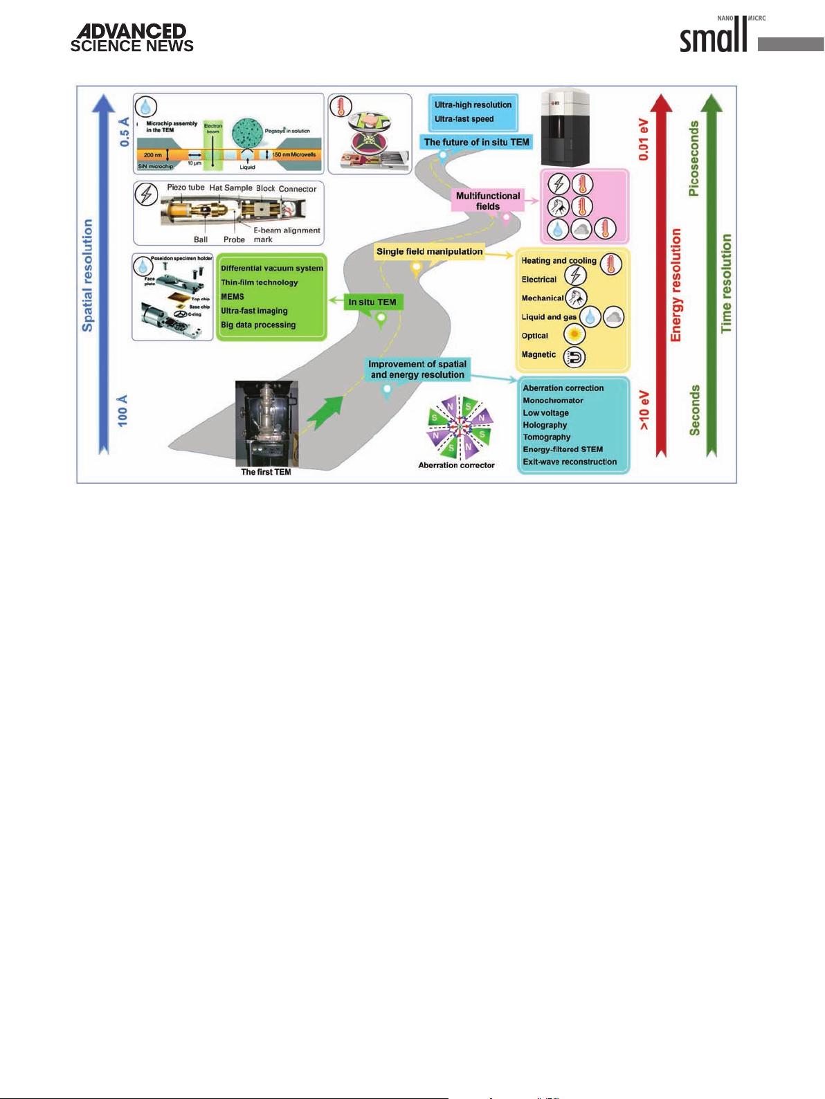
Figure 2. The chronicle of TEM: the first TEM was built by Ernst Ruska and Max Knoll in 1931; the spherical aberration corrector was developed
with sub-angstrom resolution in 2000; the evolution trends of dynamic observation of nanomaterials by in situ TEM, including thermal, electrical,
mechanical, liquid/gas environmental, optical excitation, and magnetic fields. The tendency of spatial resolution is shown on the left side, time
and energy resolutions are shown on the right side, respectively. Reproduced with permission.
[48]
Copyright 2017, Royal Society of Chemistry.
Reproduced with permission.
[49]
Copyright 2016, Cambridge University Press. The TEM machine is Titan G2 60-300.
剩余17页未读,继续阅读
2021-02-20 上传
2023-02-18 上传
2023-02-15 上传
2023-02-07 上传
2023-02-18 上传
2023-02-10 上传
2023-09-12 上传
2023-04-28 上传
2023-04-01 上传

weixin_38717031
- 粉丝: 3
- 资源: 912
 我的内容管理
展开
我的内容管理
展开


最新资源
- 新型智能电加热器:触摸感应与自动温控技术
- 社区物流信息管理系统的毕业设计实现
- VB门诊管理系统设计与实现(附论文与源代码)
- 剪叉式高空作业平台稳定性研究与创新设计
- DAMA CDGA考试必备:真题模拟及章节重点解析
- TaskExplorer:全新升级的系统监控与任务管理工具
- 新型碎纸机进纸间隙调整技术解析
- 有腿移动机器人动作教学与技术存储介质的研究
- 基于遗传算法优化的RBF神经网络分析工具
- Visual Basic入门教程完整版PDF下载
- 海洋岸滩保洁与垃圾清运服务招标文件公示
- 触摸屏测量仪器与粘度测定方法
- PSO多目标优化问题求解代码详解
- 有机硅组合物及差异剥离纸或膜技术分析
- Win10快速关机技巧:去除关机阻止功能
- 创新打印机设计:速释打印头与压纸辊安装拆卸便捷性
