TI BUF20800-Q1: 18通道伽马校正与VCOM控制器
需积分: 5 189 浏览量
更新于2024-06-28
5
收藏 1.86MB PDF 举报
TI-BUF20800-Q1是一款高性能、汽车级电压基准发生器,专为满足液晶显示器(TFT-LCD)中的伽马校正需求而设计。该设备的主要特点包括:
1. 应用兼容性:该产品符合汽车电子委员会(AEC-Q100)标准,具备一级器件温度规格,确保在严苛的汽车环境条件下稳定运行。此外,它还具备HBMESD(High-Bandwidth Multi-Gigabit Ethernet System Design)分类等级2和CDMESD分类等级C4,保证了电磁兼容性。
2. 电源效率:BUF20800-Q1具有极低的电源消耗,每通道仅为900微安,这对于电池供电的系统来说是一项优势,减少了功耗。
3. 宽工作电压范围:模拟电源输入支持7V至18V,而数字电源输入则在2V至5.5V之间,适应各种不同的电源配置。
4. 伽马校正功能:核心功能是18个可编程输出通道,用于实现精确的伽马校正,有助于改善图像质量,消除颜色偏差。
5. VCOM调节:配备两个可编程VCOM通道,每个通道提供50毫安的输出电流,允许用户调整显示面板的对比度和清晰度。
6. 高分辨率:10位分辨率使得输出电压精度高,能够精细地调整伽马曲线。
7. 轨至轨输出:这意味着输出信号可以从电源电压轨的一端直接到达另一端,提供了更宽的动态范围。
8. I2C接口:集成I2C接口,支持高达3.4MHz的高速数据传输,便于与控制电路通信。
9. 开发支持:产品附带演示板和软件,方便用户快速上手并进行原型设计。
TI-BUF20800-Q1是一款高效、灵活且功能丰富的电压基准发生器,适用于对图像质量要求高的TFT-LCD应用,如车载信息娱乐系统、医疗显示器等。使用时需注意查阅最新英文版数据手册以获取最准确的设计信息,因为尽管中文文档提供了便利,但官方英文资料始终是最权威的。
0 200 400 600 800 1000
0.6
0.4
0.2
0
−
0.2
−
0.4
−
0.6
DNL Error (LSB)
Input Code
0.6
0.4
0.2
0
−
0.2
−
0.4
−
0.6
INL Error (LSB)
0 200 400 600 800 1000
Input Code
0
10 403020 50 60 70 80 90 100
18
17
16
15
3
2
1
0
Output Voltage (V)
Output Current (mA)
OUT19, V
COM
12 (sinking)
Code =000h
V
REF L
= 1V, V
REF H
= 17..8V
R
LOAD
OUT1018 (sourcing), Code =3FFh
V
REFL REFH
= 17 V
R
LOAD
Connected to GND
OUT1018 (sin king) , Code =000 h
V
REFL REFH
= 17V
R
LOAD
Connected to 18V
OUT19, V
COM
12 (sourcing)
Code =3FFh
V
REFL
= 1 V, V
REFH
= 17..8V
R
LOAD
Connected to GND
Connected to 18V
= 0.2 V, V
= 0.2 V, V
Output Voltage (5V/div)
Time (1
m
s/div)
REFH =17V
REFL =1V
Code 3FF
→
000
Code 000
→
3FF
−
40
−
20
402010 60 80 100
Temperature ( C)°
30
25
20
15
10
5
0
Digital I
Q
(
m
A)
V
S
= 3. 3 V
V
S
= 5V
16
14
12
10
8
6
4
2
0
Analog I
Q
(mA)
−
40
−
20
402010 60 80 100
Temperature ( C)°
V
S
= 18V
V
S
= 10V
8
BUF20800-Q1
ZHCS348C –AUGUST 2011–REVISED AUGUST 2018
www.ti.com.cn
Copyright © 2011–2018, Texas Instruments Incorporated
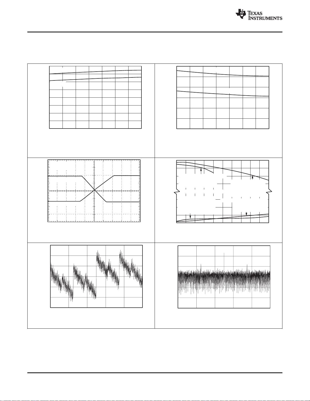
6.6 Typical Characteristics
At T
A
= 25°C, V
S
= 18 V, V
SD
= 5 V, V
REFH
= 17 V, V
REFL
= 1 V, R
L
= 1.5 kΩ connected to ground, and C
L
= 200 pF, unless
otherwise noted.
Figure 1. Analog Supply Current vs Temperature
Figure 2. Digital Supply Current vs Temperature
Figure 3. Full−scale Output Swing
Figure 4. Output Voltage vs Output Current
Figure 5. Integral Nonlinearity Error vs Input Code
Figure 6. Differential Nonlinearity Error vs Input Code
剩余41页未读,继续阅读
点击了解资源详情
点击了解资源详情
点击了解资源详情
2022-11-19 上传
2022-11-19 上传
2019-08-10 上传
2021-10-10 上传
189 浏览量
2022-11-19 上传

不觉明了
- 粉丝: 7053
- 资源: 5764
 我的内容管理
展开
我的内容管理
展开


最新资源
- app-subtags:BCP 47语言标记是从IANA子标记注册表中的子标记构建的。 此工具可帮助您查找或查找子标签并检查语言标签中的错误
- pwdhash-webextension:用于Firefox的PwdHash Webextension
- Moveit
- alloc.h头文件
- 易语言-易语言多线程例子
- a-lumen-blog
- easyrdf:EasyRdf是一个PHP库,旨在使其易于使用和产生RDF
- 数据库课程设计 网址.zip
- 关于车辆控制装置,车辆控制方法和车辆控制系统的介绍说明.rar
- 如何使用Visual Studio 2008创建用于Postgresql数据库的数据库项目?
- sk8erboyz:专案1第1组
- c51单片机 用74HC273输出数据(51/96/88/ARM)
- .net简单订票系统开发.zip
- CJL 插件实现 Js 图片旋转
- todoListW3S:W3S TodoList
- QDate
