STM32F10xxx FSFC应用笔记:驱动外部存储器指南
需积分: 10 34 浏览量
更新于2024-07-26
收藏 240KB PDF 举报
"STM32开发相关资料,包括硬件接口与软件驱动"
STM32系列单片机是基于ARM Cortex-M3或Cortex-M4内核的微控制器,因其高性能、低功耗和丰富的外设而广受欢迎。这篇应用笔记(AN2784)主要针对STM32F10xxx高密度系列的FSMC(Flexible Static Memory Controller,灵活静态存储器控制器)进行深入讲解,旨在帮助开发者利用FSMC驱动外部存储器。
FSMC是STM32F10xxx设备中的一个重要特性,它可以支持多种类型的外部存储器,如NOR Flash、NAND Flash以及SRAM等。该应用笔记首先提供了FSMC控制器的概述,详细介绍了其功能和工作原理。FSMC能够提供灵活的时序配置,适应各种外部存储器的不同接口需求。
在硬件连接部分,文档会指导如何将外部存储器正确地接入STM32F10xxx的引脚,并给出具体的硬件布局建议。这涉及到信号线的分配、电源和接地的设计,以及必要的抗干扰措施。此外,还会讨论如何计算和设置FSMC的时序参数,以确保数据传输的正确性和稳定性。
在软件方面,文档提供了使用STM32F10xx firmware library进行驱动开发的实例。这个库包含了针对不同外部存储器类型的驱动程序,例如16位异步NOR Flash、8位NAND Flash和16位异步SRAM。通过这些驱动,开发者可以轻松地在STM32上实现对各种外部存储器的读写操作。
为了便于实践,该应用笔记的示例基于STM3210E-EVAL评估板。这个板子配备了高密度STM32F10xxx器件,以及上述提到的各种外部存储器。开发者可以通过下载STM32官方网站提供的库和示例代码,进行实际的开发和测试。
这份资料对于想要使用STM32进行外部存储器扩展的开发者来说是一份宝贵的参考资料。它涵盖了从理论到实践的全过程,包括了硬件设计和软件编程的关键点,有助于提高开发效率并降低开发难度。通过学习和实践,开发者可以更好地理解和掌握STM32F10xxx的FSMC功能,从而在项目中实现更复杂、更高效的存储解决方案。
Overview of the STM32F10xxx flexible static memory controller AN2784
6/30
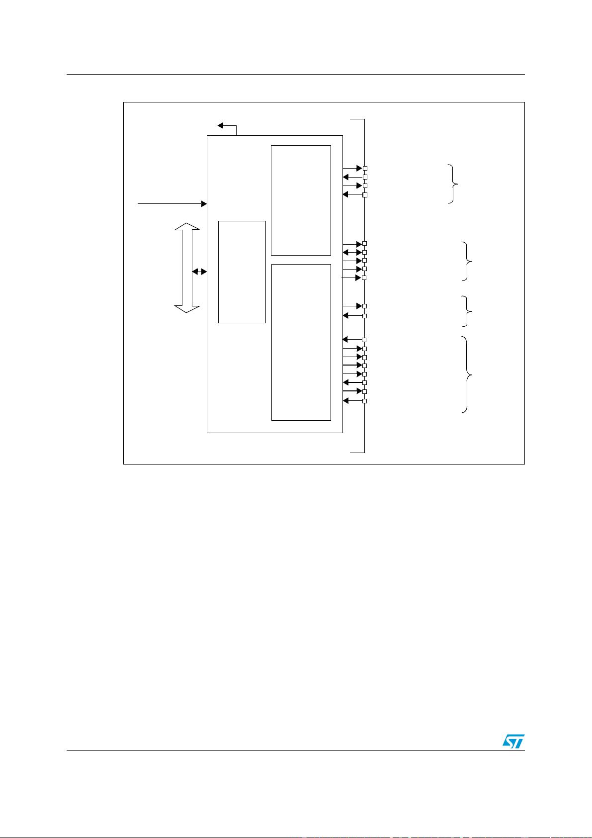
Figure 1. FSMC block diagram
From the FSMC point of view, the external memory is divided into four fixed-size banks of
256 Mbytes each, as shown in Figure 2:
● Bank 1 used by the NOR Flash/SRAM controller to address up to 4 memory devices.
This bank is split into 4 regions with 4 dedicated Chip Select signals.
● Banks 2 and 3 used by the NAND Flash/PC Card controller to address NAND Flash
devices.
● Bank 4 used by the NAND Flash/PC Card controller to address a PC Card device.
For each bank, the type of memory to be used is user-defined in the Configuration register.
AHB bus
FSMC interrupt to NVIC
NOR
HCLK
From clock
controller
controller
memory
NAND/PC Card
controller
memory
Configuration
Registers
signals
NAND
signals
Shared
signals
NOR/PSRAM
FSMC_NE[4:1]
FSMC_NL (or NADV)
FSMC_NWAIT
FSMC_A[25:0]
FSMC_D[15:0]
FSMC_NOE
FSMC_NWE
FSMC_NIORD
FSMC_NREG
FSMC_CD
signals
PC Card
ai14718
FSMC_NBL[1:0]
FSMC_NCE[3:2]
FSMC_INT[3:2]
FSMC_INTR
FSMC_NCE4_1
FSMC_NCE4_2
FSMC_NIOWR
FSMC_NIOS16
FSMC_CLK
剩余29页未读,继续阅读
2023-12-24 上传
2021-09-07 上传
2022-07-15 上传
2011-01-19 上传
2024-06-03 上传
2024-05-10 上传
2019-04-15 上传
2021-04-23 上传
2021-02-03 上传

FreesailX10i
- 粉丝: 0
- 资源: 3
 我的内容管理
展开
我的内容管理
展开


最新资源
- MATLAB实现小波阈值去噪:Visushrink硬软算法对比
- 易语言实现画板图像缩放功能教程
- 大模型推荐系统: 优化算法与模型压缩技术
- Stancy: 静态文件驱动的简单RESTful API与前端框架集成
- 掌握Java全文搜索:深入Apache Lucene开源系统
- 19计应19田超的Python7-1试题整理
- 易语言实现多线程网络时间同步源码解析
- 人工智能大模型学习与实践指南
- 掌握Markdown:从基础到高级技巧解析
- JS-PizzaStore: JS应用程序模拟披萨递送服务
- CAMV开源XML编辑器:编辑、验证、设计及架构工具集
- 医学免疫学情景化自动生成考题系统
- 易语言实现多语言界面编程教程
- MATLAB实现16种回归算法在数据挖掘中的应用
- ***内容构建指南:深入HTML与LaTeX
- Python实现维基百科“历史上的今天”数据抓取教程
