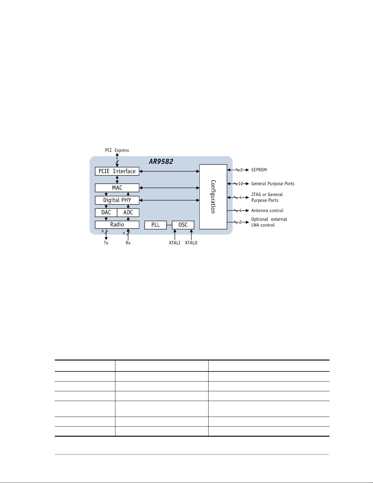
18 • AR9582 Single-Chip 2x2 MIMO MAC/BB/Radio for 802.11n WLANs Atheros Communications, Inc.
18 • December 2011 COMPANY CONFIDENTIAL
2.1.3 On-Chip One-Time Programmable (OTP)
Memory
The AR9582 provides OTP memory for storing
calibration data to eliminate the need for an
external EEPROM. The hardware detects
whether an external EEPROM is present. If
none is present, it sets bit [8] of the “EEPROM
Control (HOST_INTF_EEPROM_CTRL)”
register is set to one.
2.1.4 Serial EEPROM Interface
The AR9582 provides a serial interface to access
an external EEPROM. The EEPROM interface
modifies configuration space registers and
configuration- and vendor-specific
information.
The off-chip EEPROM can be:
■
A 32-Kb device, organized as 2,048 entries
of 16 bits each (2,048x16)
■
An 64-Kb device, organized as 4,096 entries
of 16 bits each (4,096x16)
The hardware automatically detects EEPROM
size. The EEPROM addressing is 16 bits wide,
with each 16-bit EEPROM mapped into the
AR9582's register space. Each 32-bit aligned
address corresponds to a unique EEPROM
location. Because the host interface supports
32-bit register accesses and ignores the two
least significant address bits, the address offset
provided by the host interface corresponds to
four times the EEPROM location.
At reset, some PCI Express configuration
registers load from the EEPROM while others
are programmed by the host or initialized by
AR9582 hardware. To ensure that the EEPROM
contents are valid, a 16-bit word at address
offset 0x2000 is checked. If the values do not
match 0xA55A, the EEPROM contents are
ignored and the default values loaded.
2.1.5 EEPROM Auto-Sizing Mechanism
The first procedure after reset is to read the
offset address 0x2000 to check for the content
0xA55A. The EEPROM physical presence,
programmed state, and size are determined
automatically. If the offset address 0x2000
contents do not match the 0xA55A value for
any supported EEPROM sizes, the AR9582
assumes the EEPROM is not present on the
PCB, or is present but not programmed. In
either case, the logic uses the default values as
described in “Serial EEPROM Interface”.
2.1.6 EEPROM Read/Write Protection
Mechanism
The EEPROM contains a 16-bit word protect
mask value at address location 0x2010H that
prevents software from accessing certain
regions. The mask is 16 bits wide and contains
eight sub-masks that are 2 bits wide.
The sub-mask can have four values that
determine the access types permitted to the
associated protection region:
■
00: Read/write access allowed
■
01: Write-only access allowed
■
10: Read-only access allowed
■
11: No access allowed
2.2 Reset
The RESET_L pin controls the AR9582 chip
reset. The AR9582 host interface receives two
reset signals as below:
■
RESET_L pin
Controls the AR9582 power reset
■
PCIE_RST_L
Controls the PCI Express core reset
In addition, the real-time clock (RTC) reset
register provides software control of warm
reset for the MAC/baseband and PCU blocks.
See the register “RTC Reset and Force Sleep
and Force Wakeup (RTC_RESET)” on page 108.
2.3 GPIO
The AR9582 provides 13 configurable bi-
directional general purpose I/O ports and 1
configurable input-only port. Each GPIO port
can be configured independently as input or
output using the GPIO control registers.
Information presented at GPIO inputs and
outputs can be read from the “GPIO Output
(HOST_INTF_GPIO_OUT)” and “GPIO Input
(HOST_INTF_GPIO_IN)” registers.
In addition, Bluetooth coexistence functions
can also map to GPIO10, GPI9, and GPIO[7:0].
See the “GPIO Input MUX1
(HOST_INTF_GPIO_INPUT_MUX1)” and
“GPIO Input MUX2
(HOST_INTF_GPIO_INPUT_MUX2)”
registers. Table 6-14 on page 102 lists the
functionalities that can map to GPIO outputs
using the “GPIO Output MUX1
(HOST_INTF_GPIO_OUTPUT_MUX1)”,
“GPIO Output MUX2
(HOST_INTF_GPIO_OUTPUT_MUX2)”, and
“GPIO Output MUX3
(HOST_INTF_GPIO_OUTPUT_MUX3)”
registers.


