DDR3L Device Operation
16
1.4.3.1 DLL Enable/Disable
MR1 (A0 = 0), the DLL is automatically disabled when entering Self-Refresh operation and is automatically
re-enabled upon exit of Self-Refresh operation. Any time the DLL is enabled and subsequently reset, tDLLK
clock cycles must occur before a Read or synchronous ODT command can be issued to allow time for the
internal clock to be synchronized with the external clock. Failing to wait for synchronization to occur may
result in a violation of the tDQSCK, tAON or tAOF parameters. During tDLLK, CKE must continuously be reg
-
istered high. DDR3 SDRAM does not require DLL for any Write operation, except when RTT_WR is enabled
and the DLL is required for proper ODT operation. For more detailed information on DLL Disable operation
refer to "2.5 DLL-off Mode" on page 25.
The direct ODT feature is not supported during DLL-off mode. The on-die termination resistors must be dis-
abled by continuously registering the ODT pin low and/or by programming the RTT_Nom bits MR1{A9,A6,A2}
to {0,0,0} via a mode register set command during DLL-off mode.
The dynamic ODT feature is not supported at DLL-off mode. User must use MRS command to set Rtt_WR,
MR2 {A10, A9} = {0,0}, to disable Dynamic ODT externally.
1.4.3.2 Output Driver Impedance Control
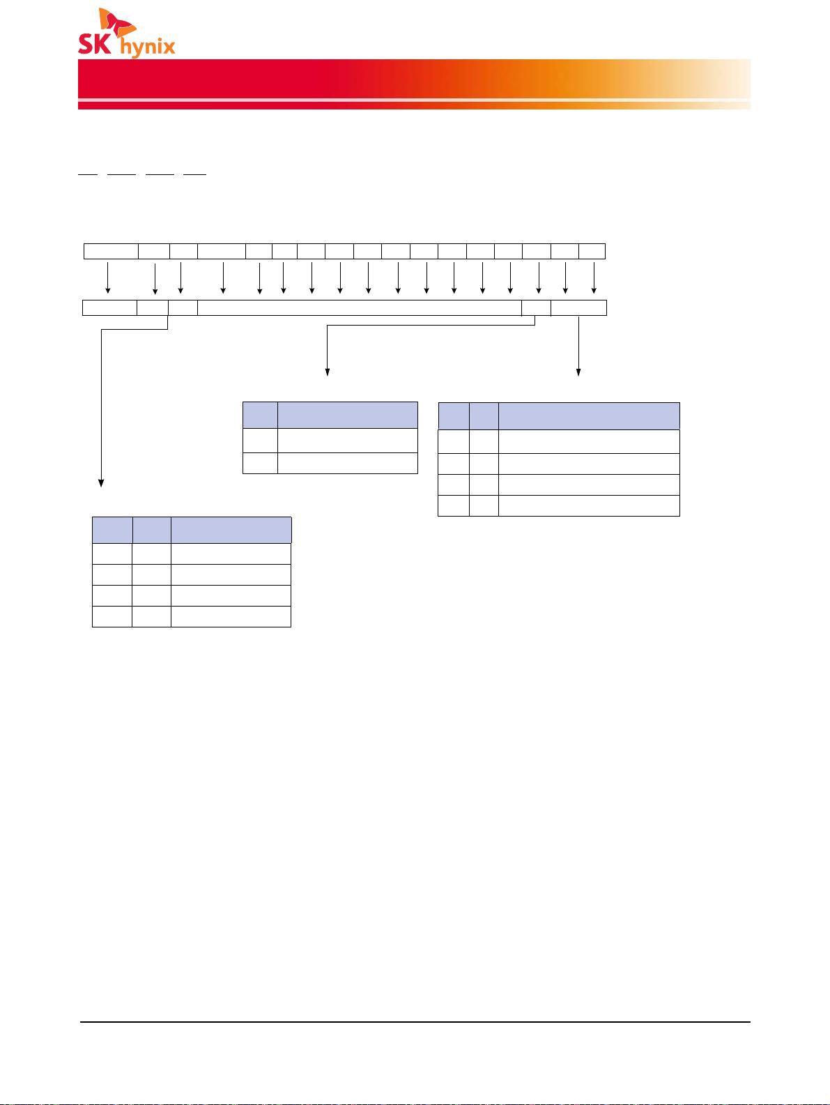
The output driver impedance of the DDR3 SDRAM device is selected by MR1 (bits A1 and A5) as shown in
Figure 7.
1.4.3.3 ODT Rtt Values
DDR3 SDRAM is capable of providing two different termination values (Rtt_Nom and Rtt_WR). The nominal
termination value Rtt_Nom is programmed in MR1. A separate value (Rtt_WR) may be programmed in MR2
to enable a unique RTT value when ODT is enabled during writes. The Rtt_WR value can be applied during
writes even when Rtt_Nom is disabled.
1.4.3.4 Additive Latency (AL)
Additive Latency (AL) operation is supported to make command and data bus efficient for sustainable band-
widths in DDR3 SDRAM. In this operation, the DDR3 SDRAM allows a read or write command (either with or
without auto-precharge) to be issued immediately after the active command. The command is held for the
time of the Additive Latency (AL) before it is issued inside the device. The Read Latency (RL) is controlled by
the sum of the AL and CAS Latency (CL) register settings. Write Latency (WL) is controlled by the sum of the
AL and CAS Write Latency (CWL) register settings. A summary of the AL register options are shown in
Table 3.
NOTE: AL has a value of CL - 1 or CL - 2 as per the CL values programmed in the MR0 register.
1.4.3.5 Write leveling
For better signal integrity, DDR3 memory module adopted fly-by topology for the commands, addresses,
control signals, and clocks. The fly-by topology has the benefit of reducing the number of stubs and their
length, but it also causes flight time skew between clock and strobe at every DRAM on the DIMM. This makes
it difficult for the Controller to maintain tDQSS, tDSS, and tDSH specification. Therefore, the DDR3 SDRAM
supports a ‘write leveling’ feature to allow the controller to compensate for skew.
See "2.8 Write Leveling" on
page 30 for more details.
Table 3: Additive Latency (AL) Settings
A4 A3 AL
0 0 0 (AL Disabled)
0 1 CL - 1
1 0 CL - 2
1 1 Reserved


