GaN器件在空间级高可靠性正向转换器中的实际效益
需积分: 0 186 浏览量
更新于2024-08-03
收藏 5.11MB PDF 举报
随着科技的进步,氮化镓(Gallium Nitride, GaN)器件因其卓越的性能和高效率,在航天领域的应用越来越受到关注。本文发表在《电气与电子工程师学会新兴和精选电力电子期刊》(IEEE Journal of Emerging and Selected Topics in Power Electronics)上,于2022年10月第10卷第5期,探讨了GaN器件如何在高可靠性正向转换器中发挥作用,特别是在空间飞行器中,其传统 MOSFET 技术所面临的辐射硬性限制是一个关键挑战。
尽管目前市场上辐射硬化的(GaN)高电子迁移率晶体管(GaN High Electron Mobility Transistor, HEMT)数量有限,但它们已经显示出显著的优势,可以提高空间级转换器的效率和功率密度。然而,GaN技术的研究常常侧重于未来潜在应用,将GaN用于已经成熟并经过空间认证的设计并不常见。本文的焦点在于评估现市可用的、经过空间等级认证的GaN HEMTs在异步正向转换器中的实际效益,这种转换器在隔离的、中等功率的直流-直流变换器中广泛采用,适用于各种卫星和其他空间设备。
正向转换器,特别是异步设计,对于航天器而言是至关重要的,因为它支持在不同电源条件下提供稳定的电压和电流。传统的硅基MOSFET由于其对辐射的敏感性,在太空环境中面临性能衰退的问题。而GaN HEMTs则展现出更好的抗辐射特性,能够在辐射环境下保持稳定的工作状态,从而确保系统的长期可靠性和性能。
作者Aidan Phillips、Thomas Cook(学生会员,IEEE)、Brian West 和 Brandon M. Grainger(资深会员,IEEE)通过严谨的实验和分析,量化了GaN HEMTs在提高转换效率、减少散热需求、以及减小系统尺寸方面的具体优势。他们的研究不仅提供了对现有GaN器件在空间应用中的实际效能评估,还为未来的空间级电源转换设计提供了有价值的参考依据,鼓励了业界在更广泛应用GaN技术的同时,进一步优化其在空间环境中的可靠性和效率提升。
PHILLIPS et al.: GaN EFFICACY FOR HIGH-RELIABILITY FORWARD CONVE RTERS IN SPACECRAFT 5359
as other loss modes should be normalized across the two194
boards. Lossy snubber networks affected by the switch are195
of high interest.196
In this article, several definitions for various sets of devices197
will be used. “COTS devices,” as defined above, consist of198
devices that are readily available to keep costs down for ter-199
restrial prototypes. “Rad-hard devices” are significantly more200
costly than COTS components due to their design and quali-201
fications for space environments. “Error bounding COTS” are202
devices that do not match with any available rad-hard part but203
are used to error bound the available devices to a maximum204
performance range. Finally, a “matched optimal FET” is a205
COTS FET with similar performance on Earth as its rad-hard206
equivalent.207
III. TOPOLOGY SELECTION AND208
SPECIFICATION JUSTIFICATION209
The specifications for the dc–dc converter used in this exper-210
iment follow common requirements found in NASA satellite211
systems. Solar arrays and their corresponding battery banks212
provide a nominally 28-V dc bus voltage for many satellites,213
which then requires isolated dc–dc conversion to power space-214
craft computing, sensing, actuation, communication, and other215
critical loads. The forward converter topology dominates the216
market available rad-hard isolated power supplies, making it a217
useful platform for this study. In addition, the increase in GaN218
power device research in the context of low-power, point-of-219
load converters [17] makes the choice of an isolated, medium-220
power topology more desirable.221
Furthermore, since the experiment centers around the effect222
of emerging transistor technology, there is no need for a223
novel or niche converter topology. Choosing a common, well-224
understood topology follows the theme of practicality and225
generality in this research. That said, the c hosen converter226
should reflect the degree of complexity that is being employed227
to capture valuable efficiency gains in modern aerospace con-228
verters. Also, the risks and lack of flight heritage that make229
zero voltage/current switching or resonant-based converters a230
rare selection for high-reliability designs will eliminate them231
as candidates in this experiment.232
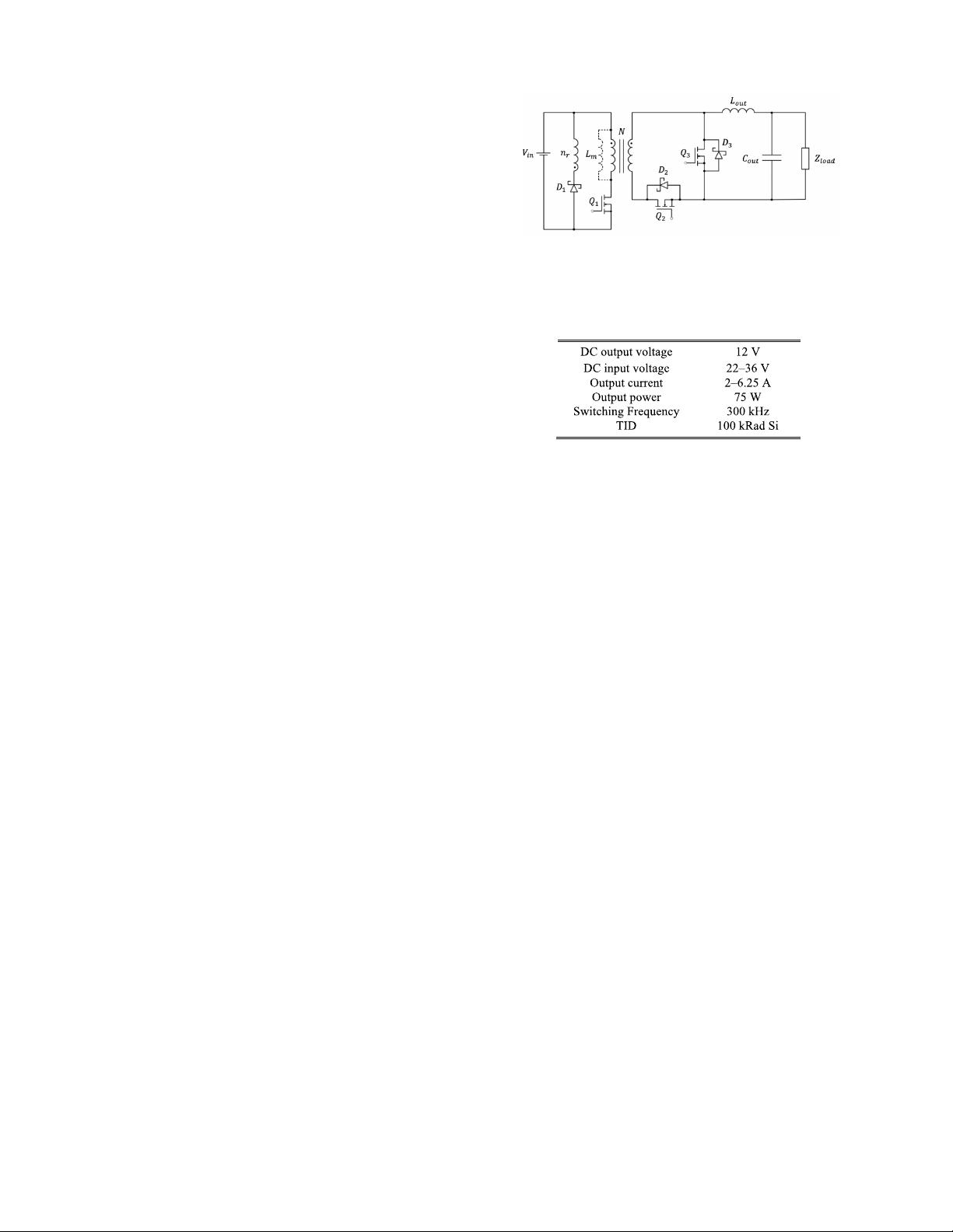
With these considerations, a synchronously rectified, reset233
winding forward converter was selected, as shown in Fig. 1.234
The forward converter was chosen over a flyback due to its235
market dominance and nonpulsating secondary current, which236
is desirable for loss mitigation and EMI minimization when237
entering the medium-power regime at low voltage. The syn-238
chronous rectification requires significant coordination strate-239
gies over the isolation barrier such that the desired complexity240
requirement is met. The use of a reset winding further sepa-241
rates the co nverter from a reliance on part parasitics, which242
aids in co nsistency and reliability.243
Shown in Table I are the six primary design specifications.244
The input voltage range is standard for the mentioned 28-V245
bus satellite systems. The maximum power specification was246
set to push the design into the medium-power region.247
Switching frequency selection is constrained by the PWM248
controller, maximum duty cycle, and predicted GaN benefits.249
Fig. 1. Synchronous forward converter topology with reset winding.
TABLE I
FORWARD CONVERTER DES IGN SPECI FICATI ONS
GaN technology promises an increase in power density with- 250
out the loss in efficiency that comes with higher switching 251
frequencies in hard switched applications. However, when 252
using rad-hard PWM controllers, the upper bound on switching 253
frequency typically falls at the 500-kHz point. Though there 254
are exceptions for PWM controllers that fit isolated designs, 255
including ASIC or FPGA-driven solutions, they do not repre- 256
sent the largest class of converter controllers that have obtained 257
flight heritage. Further more, the oscillator circuits that set 258
switching frequency within a PWM controller often make a 259
tradeoff for the duty cycle. The current source that discharges 260
the externally set RC network for the oscillator is fixed in 261
magnitude such that, as the switching frequency increases, the 262
maximum duty cycle must decrease. For a forward converter, 263
a reduction in the maximum duty cycle can lead to an increase 264
in the transformer turns ratio and a subsequent increase in the 265
peak voltages o n the primary and secondary switches, which 266
limits part selection and performance. 267
The choice of switching frequency is also constrained by the 268
design of the experiment. If too low, then the strengths of GaN 269
may not be seen. If too high, then the claim of a reasonable 270
operating point for the b oard that uses traditional silicon 271
MOSFETs will disappear due to excess switching losses. The 272
chosen 300-kHz specification meets the ability of the PWM 273
controller while giving the GaN device enough degrees of 274
freedom and the Si MOSFETs a m anageable operating point 275
from a loss perspective. 276
The TID specification can be seen as a restriction on all 277
the converter components. This cumulative radiation metric 278
contributes to the lifetime of the converter and is a tenant of 279
space qualification. 280
IV. CONVERTER DESIGN AND COMPONENT SELECTION 281
Forward converter design methodology can be found 282
in numerous industry application notes and textbook 283
resources [18]. The equations and design decisions detailed in 284
this section are meant to further classify the converter so that 285
Authorized licensed use limited to: ShanghaiTech University. Downloaded on May 01,2024 at 11:09:49 UTC from IEEE Xplore. Restrictions apply.
剩余13页未读,继续阅读
2018-12-12 上传
2021-08-29 上传
2023-04-02 上传
2023-07-12 上传
2023-07-08 上传
2023-04-28 上传
2023-07-08 上传
2023-10-14 上传
2023-07-14 上传

北行黄金橘
- 粉丝: 3984
- 资源: 4
 我的内容管理
展开
我的内容管理
展开


最新资源
- 十种常见电感线圈电感量计算公式详解
- 军用车辆:CAN总线的集成与优势
- CAN总线在汽车智能换档系统中的作用与实现
- CAN总线数据超载问题及解决策略
- 汽车车身系统CAN总线设计与应用
- SAP企业需求深度剖析:财务会计与供应链的关键流程与改进策略
- CAN总线在发动机电控系统中的通信设计实践
- Spring与iBATIS整合:快速开发与比较分析
- CAN总线驱动的整车管理系统硬件设计详解
- CAN总线通讯智能节点设计与实现
- DSP实现电动汽车CAN总线通讯技术
- CAN协议网关设计:自动位速率检测与互连
- Xcode免证书调试iPad程序开发指南
- 分布式数据库查询优化算法探讨
- Win7安装VC++6.0完全指南:解决兼容性与Office冲突
- MFC实现学生信息管理系统:登录与数据库操作
