Analog Dialogue 46-12, December (2012) 1
Front-End Amplier and
RC Filter Design for a
Precision SAR Analog-to-
Digital Converter
By Alan Walsh
Successive-approximation (SAR) ADCs offer high resolution,
excellent accuracy, and low power consumption. Once a particular
precision SAR ADC has been chosen, system designers must deter-
mine the support circuitry needed to obtain the best results. The
three principal areas to consider are the front end, which interfaces
the analog input signal to the ADC, the voltage reference, and the
digital interface. This article focuses on the circuit requirements
and trade-offs in designing the front end. Useful information on
the other areas, which are device- and system-specic, can be
found in data sheets—and in this article’s references.
The front end consists of two parts: the driving amplier and the
RC lter. The amplier conditions the input signal—as well as
acting as a low-impedance buffer between the signal source and
the ADC input. The RC lter limits the amount of out-of-band
noise arriving at the ADC input and helps to attenuate the kick
from the switched capacitors in the ADC’s input.
Choosing the right amplier and RC lter for a SAR ADC
can be a challenge, especially when the application needs to
differ from the routine data sheet usage of the ADC. Looking
at the various application factors that inuence amplier and
RC choice, we provide design guidelines that lead to the best
solution. Major considerations include input frequency, throughput,
and input multiplexing.
Selecting a Suitable RC Filter
To select a suitable RC lter, we must calculate the RC bandwidth
for single-channel or multiplexed applications, then select values
for R and C.
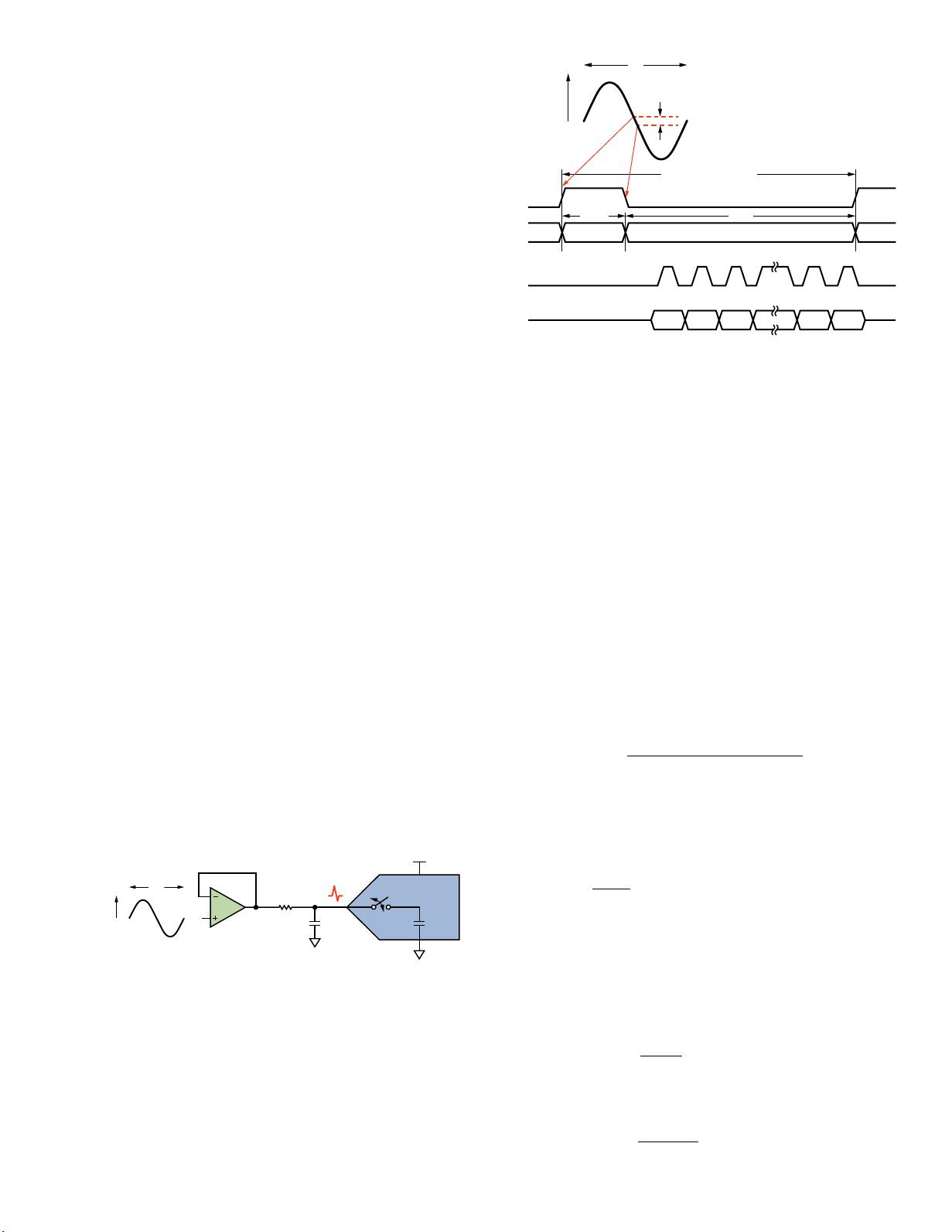
Figure 1 shows a typical amplier, single-pole RC lter, and
ADC. The ADC input presents a switched-cap load to the driving
circuitry. Its 10-MHz input bandwidth means that low-noise is
needed over a wide bandwidth to get a good signal-to-noise ratio
(SNR). The RC network limits the bandwidth of the input signal
and reduces the amount of noise fed to the ADC by the amplier
and upstream circuitry. Too much band limiting will increase the
settling time and distort the input signal, however.
V
REF
C
DAC
R
EXT
C
EXT
V
PEAK
t
CONV
t
ACQ
KICK
f
IN
f
IN
Figure 1. Typical amplier, RC lter, and ADC.
The minimum RC value needed to settle the ADC input while
also optimally band limiting the noise can be calculated assuming
exponential settling of a step input. To calculate the size of the step,
we need to know the input signal frequency, amplitude, and ADC
conversion time. The conversion time, t
CONV
(Figure 2), is when the
capacitive DAC is disconnected from the input and is performing
bit trials to generate the digital code. At the end of the conversion
time, the capacitive DAC, which holds the previous sample charge,
is switched back to the input. This step change represents how
much the input signal has changed in that time. The time taken
to settle this step is known as the reverse settling time.
www.analog.com/analogdialogue
1 2 3 N
–
2
CONVERSIONACQUISITION ACQUISITION
CNV
SCK
SDO
N
–
1 N
D
N
D
1
D
0
D
N
–
1
D
N
–
2
t
ACQ
VOLTAGE STEP
V
PEAK
f
IN
ADC THROUGHPUT t
SR
t
CONV
Figure 2. Typical timing diagram for N-bit ADC.
The maximum undistorted rate of change of a sine wave signal
with a given input frequency can be calculated as
If the conversion rate of the ADC is considerably higher than
the maximum input frequency, the maximum amount the input
voltage has changed during the conversion time is given by
This is the maximum voltage step that is seen by the capacitive
DAC when it is switched back to acquire mode. This step is then
attenuated by the parallel combination of the DAC’s capacitance
and that of the external capacitor. For this reason, it is important
that the external capacitor be relatively large—a few nanofarads.
This analysis will assume that the on resistance of the input switch
has a negligible effect. The step size that now needs to be settled
is given by
=
IN
PEAK
CONV
DAC
STEP
Next, calculate the time constant to settle the ADC input to ½ LSB
during the acquisition time of the ADC. Assuming exponential
settling of the step input, the required RC time constant, τ, is
=
ACQ
N
where t
ACQ
is the acquisition time and N
TC
is the number of
time constants required to settle. The number of time constants
required can be calculated from the natural logarithm of the
ratio of the step size, V
ST E P
, to the settling error—which in this
case is ½ LSB,
=
N + 1
REF
half_lsb
giving
N
TC
= ln
V
STEP
V
half_lsb


