超低抖动LMK61PD0A2振荡器:高性能 PLL 解决方案
需积分: 9 133 浏览量
更新于2024-06-28
4
收藏 1.31MB PDF 举报
TI-LMK61PD0A2是一款高性能、超低噪声的振荡器,专为替换晶体振荡器、SAW振荡器或芯片振荡器而设计,特别适用于对低抖动有极高要求的应用领域。该器件具有以下关键特性:
1. **低抖动性能**:在高达100MHz的输出频率下,典型抖动值仅为90 femtoseconds (fs),确保了信号传输的极高稳定性,适用于如开关、路由器、网卡、BBU、服务器和存储设备等对时钟精确性的敏感设备。
2. **电源抑制比(PSRR)优良**:LMK61PD0A2能提供卓越的电源干扰抑制,达到-70分贝耦合噪声抑制比,对于噪声敏感的测试与测量、医疗成像等应用非常理想。
3. **灵活输出频率和格式**:用户可以根据需要选择多种频率选项,包括62.5MHz、100MHz、106.25MHz、125MHz、156.25MHz、212.5MHz和312.5MHz,输出格式支持LVPECL、LVDS和HSTL,提供高度定制化能力。
4. **预编程的内部存储器**:振荡器内置了多组预设的启动配置,通过调整FS[1:0]引脚,可以快速选择七种不同的基准时钟频率,方便快捷。
5. **宽工作电压和温度范围**:3.3V工作电压设计,能在工业温度范围内(-40°C至+85°C)稳定运行,确保设备在各种环境下的可靠性能。
6. **接口兼容性**:OS引脚设计灵活,可通过配置为VDD、GND或NC来选择相应的输出格式,适应不同系统接口需求。
7. **小型封装**:采用紧凑的7mmx5mm 8引脚封装,节省空间的同时便于集成到电路板设计中。
TI-LMK61PD0A2是一款功能强大、灵活性高的超低抖动振荡器,广泛应用于需要高精度时钟的现代电子设备中,无论是通信设备还是医疗设备,都能提供出色的性能支持。为了充分利用这款产品的优势,开发者应参考技术文档、工具软件和社区支持,确保正确地应用和调试。
LMK61PD0A2
ZHCSEB9A –OCTOBER 2015–REVISED NOVEMBER 2015
www.ti.com.cn
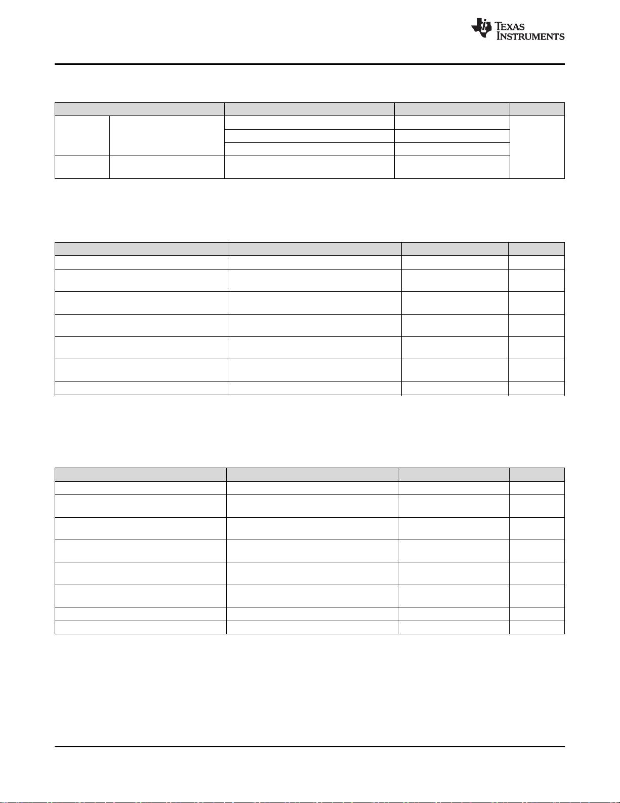
7.5 Electrical Characteristics - Power Supply
(1)
VDD = 3.3 V ± 5%, T
A
= -40C to 85°C
PARAMETER TEST CONDITIONS MIN TYP MAX UNIT
IDD Device Current Consumption LVPECL
(2)
162 208 mA
LVDS 152 196
HCSL 155 196
IDD-PD Device Current Consumption OE = GND 136
when output is disabled
(1) Refer to Parameter Measurement Information for relevant test conditions.
(2) On-chip power dissipation should exclude 40 mW, dissipated in the 150 ohm termination resistors, from total power dissipation.
7.6 LVPECL Output Characteristics
(1)
VDD = 3.3 V ± 5%, T
A
= -40C to 85°C
PARAMETER TEST CONDITIONS MIN TYP MAX UNIT
f
OUT
Output Frequency
(2)
62.5 312.5 MHz
V
OD
Output Voltage Swing 700 800 1200 mV
(V
OH
- V
OL
)
(2)
V
OUT, DIFF, PP
Differential Output Peak-to- 2 x V
Peak Swing |V
OD
|
V
OS
Output Common Mode VDD – V
Voltage 1.55
t
R
/ t
F
Output Rise/Fall Time (20% to 120 200 ps
80%)
(3)
PN-Floor Output Phase Noise Floor 156.25 MHz -165 dBc/Hz
(f
OFFSET
> 10 MHz)
ODC Output Duty Cycle
(3)
45% 55%
(1) Refer to Parameter Measurement Information for relevant test conditions.
(2) An output frequency over f
OUT
max spec is possible, but output swing may be less than V
OD
min spec.
(3) Ensured by characterization.
7.7 LVDS Output Characteristics
(1)
VDD = 3.3 V ± 5%, T
A
= -40°C to 85°C
PARAMETER TEST CONDITIONS MIN TYP MAX UNIT
f
OUT
Output Frequency
(1)
62.5 312.5 MHz
V
OD
Output Voltage Swing 300 390 480 mV
(V
OH
- V
OL
)
(1)
V
OUT, DIFF, PP
Differential Output Peak-to- 2 x V
Peak Swing |V
OD
|
V
OS
Output Common Mode 1.2 V
Voltage
t
R
/ t
F
Output Rise/Fall Time (20% to 150 250 ps
80%)
(2)
PN-Floor Output Phase Noise Floor 156.25 MHz -162 dBc/Hz
(f
OFFSET
> 10 MHz)
ODC Output Duty Cycle
(2)
45% 55%
R
OUT
Differential Output Impedance 125 Ohm
(1) An output frequency over f
OUT
max spec is possible, but output swing may be less than V
OD
min spec.
(2) Ensured by characterization.
6 Copyright © 2015, Texas Instruments Incorporated
剩余26页未读,继续阅读
2022-11-30 上传
2022-11-30 上传
2022-11-30 上传
2022-11-30 上传
2022-11-30 上传
2022-11-30 上传
2022-11-30 上传
2022-11-30 上传
2022-11-30 上传

不觉明了
- 粉丝: 3800
- 资源: 5759
 我的内容管理
展开
我的内容管理
展开


最新资源
- StarModAPI: StarMade 模组开发的Java API工具包
- PHP疫情上报管理系统开发与数据库实现详解
- 中秋节特献:明月祝福Flash动画素材
- Java GUI界面RPi-kee_Pilot:RPi-kee专用控制工具
- 电脑端APK信息提取工具APK Messenger功能介绍
- 探索矩阵连乘算法在C++中的应用
- Airflow教程:入门到工作流程创建
- MIP在Matlab中实现黑白图像处理的开源解决方案
- 图像切割感知分组框架:Matlab中的PG-framework实现
- 计算机科学中的经典算法与应用场景解析
- MiniZinc 编译器:高效解决离散优化问题
- MATLAB工具用于测量静态接触角的开源代码解析
- Python网络服务器项目合作指南
- 使用Matlab实现基础水族馆鱼类跟踪的代码解析
- vagga:基于Rust的用户空间容器化开发工具
- PPAP: 多语言支持的PHP邮政地址解析器项目
