VHDL驱动的RISC微处理器设计:流水线与数据冒险解决
需积分: 9 2 浏览量
更新于2024-07-06
收藏 2.04MB PDF 举报
本篇作业报告主要探讨了基于VHDL的RISC微处理器设计,着重于利用指令流水线技术来提升计算性能。在设计过程中,作者Si Yue Zhang选择了计算机硬件与数字设计作为研究背景,采用RISC( Reduced Instruction Set Computing,精简指令集计算机)微处理器的核心部分作为设计目标。核心结构包括解码器、RAM和算术逻辑单元(ALU),它们共同完成基本的32位变量操作、调用和存储任务。
首先,ALU的设计和测试是微处理器实现的关键组件,负责执行各种算术和逻辑运算。ALU的设计不仅要满足功能需求,还要通过VHDL进行有效的编码和验证。接下来,报告提及将ROM升级为RAM,以提供更快的数据访问速度,这是处理器性能优化的一个重要步骤。
解码器的设计是处理器理解和解释指令的第一步,它决定了如何将输入的二进制代码转化为具体的操作。同时,RAM的测试和改进确保数据能够快速准确地存储和检索,这对于流水线工作流程至关重要。
在设计中引入了指令流水线,这是现代处理器提高效率的关键策略。流水线包括多个阶段,如指令获取、指令解码、操作执行、结果存储等。报告详细讨论了流水线原理,包括挑战如数据冒险(当多个指令访问同一数据时可能导致的延迟)、无操作(No-op)指令的作用以及数据转发机制,这些都是为了克服并行执行中的潜在问题。
重排序(Reordering Pipeline)是流水线策略的一部分,用于解决不同指令执行时间不一致导致的问题,确保正确的指令顺序执行。通过这种技术,处理器能够在不影响最终结果的前提下优化资源利用率。
最后,报告展示了设计过程中的成果,包括截图和实际运行处理器的步骤,这证明了基于VHDL的RISC微处理器设计的成功实施。
总结来说,这篇论文深入剖析了VHDL在RISC微处理器设计中的应用,涵盖了硬件实现、流水线设计策略以及实际操作验证等多个关键环节,为理解现代计算机体系结构提供了深入的学习资料。
Siyue Zhang
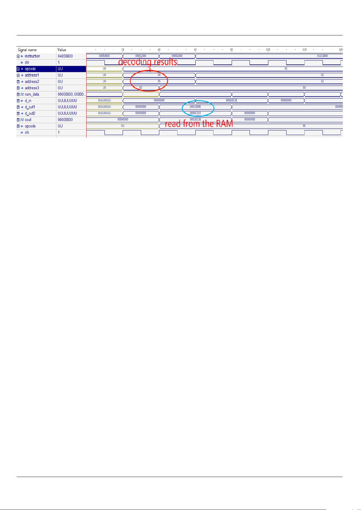
Figure 4: Testbench for the RAM and Decoder
"01011" after 200ns, "01100" after 220ns,
"01101" after 240ns, "01110" after 260ns,
"01111" after 280ns;
The result of running the testbench for ROM is shown in figure 3. As
we can see from the result, the output of the RAM is exactly the initial
value corresponding to their addresses, so that we prove our ROM entity
is correct.
3 DECODER AND RAM
3.1 Design of Decoder
Decoder can break the long 32-bit instructions into short pieces and each
piece of instruction is the required component to feed to the ALU and
the RAM. The format of these instructions is as follows: The first 6 bits
identify the opcode; The next 5 bits identify first source register; The next
5 bits identify second source register; The next 5 bits identify destination
register; The final 11 bits are unused. So the design of the decoder is
simply reassigning the instruction, and we also need to add pipeline and
let the decoder breaks one instruction every clock cycle.
process (clk)
begin
if (rising_edge(clk)) then
opcode <= instruction(31 downto 26);
address1 <= instruction(25 downto 21);
address2 <= instruction(20 downto 16);
address3 <= instruction(15 downto 11);
end if;
end process;
3.2 Upgrade ROM to RAM
Comparing to ROM, RAM can be changed by user and have both read
and write ports. Therefore we simply add a newline of code on the ROM:
process (clk)
begin
if (rising_edge(clk)) then
ram_data( CONV_INTEGER(address3) ) <= din;
end if;
end process;
where the ”din” is the data you want to store in the RAM, and address
tells the RAM where do you want to save the data.
3.3 Testing the RAM and Decoder
To test the correctness of RAM and decoder, we use a series of
instructions: r2=r4+r5, r3=r4+r5, r3=r1+r2:
3
剩余14页未读,继续阅读
2013-12-06 上传
120 浏览量
2020-10-24 上传
2020-12-08 上传
2023-06-22 上传
2022-09-22 上传
2019-04-04 上传
点击了解资源详情
点击了解资源详情

章靓
- 粉丝: 4
- 资源: 1
 我的内容管理
展开
我的内容管理
展开


最新资源
- Java集合ArrayList实现字符串管理及效果展示
- 实现2D3D相机拾取射线的关键技术
- LiveLy-公寓管理门户:创新体验与技术实现
- 易语言打造的快捷禁止程序运行小工具
- Microgateway核心:实现配置和插件的主端口转发
- 掌握Java基本操作:增删查改入门代码详解
- Apache Tomcat 7.0.109 Windows版下载指南
- Qt实现文件系统浏览器界面设计与功能开发
- ReactJS新手实验:搭建与运行教程
- 探索生成艺术:几个月创意Processing实验
- Django框架下Cisco IOx平台实战开发案例源码解析
- 在Linux环境下配置Java版VTK开发环境
- 29街网上城市公司网站系统v1.0:企业建站全面解决方案
- WordPress CMB2插件的Suggest字段类型使用教程
- TCP协议实现的Java桌面聊天客户端应用
- ANR-WatchDog: 检测Android应用无响应并报告异常
