MSP430FR5739-EP
ZHCSD33A –NOVEMBER 2014–REVISED DECEMBER 2014
www.ti.com.cn
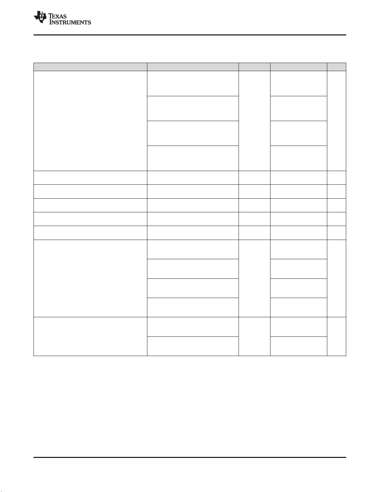
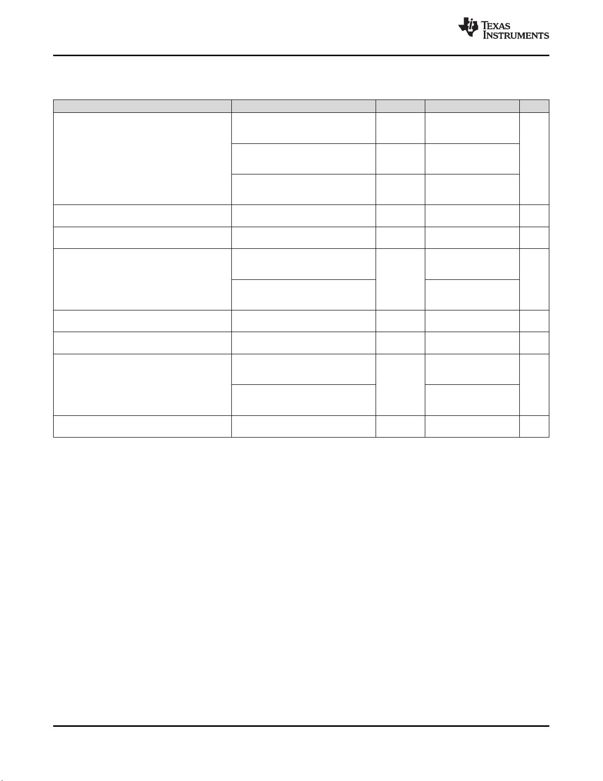
4.12 Crystal Oscillator, XT1, Low-Frequency (LF) Mode
(1)
over recommended ranges of supply voltage and operating free-air temperature (unless otherwise noted)
(2)
PARAMETER TEST CONDITIONS V
CC
MIN TYP MAX UNIT
ƒ
OSC
= 32768 Hz, XTS = 0,
XT1BYPASS = 0, XT1DRIVE = {1}, 3 V 60
C
L,eff
= 9 pF, T
A
= 25°C,
Additional current consumption ƒ
OSC
= 32768 Hz, XTS = 0,
ΔI
VCC.LF
XT1 LF mode from lowest drive XT1BYPASS = 0, XT1DRIVE = {2}, 3 V 90 nA
setting T
A
= 25°C, C
L,eff
= 9 pF
ƒ
OSC
= 32768 Hz, XTS = 0,
XT1BYPASS = 0, XT1DRIVE = {3}, 3 V 140
T
A
= 25°C, C
L,eff
= 12 pF
XT1 oscillator crystal frequency,
ƒ
XT1,LF0
XTS = 0, XT1BYPASS = 0 32768 Hz
LF mode
XT1 oscillator logic-level square-
ƒ
XT1,LF,SW
XTS = 0, XT1BYPASS = 1
(3) (4)
10 32.768 50 kHz
wave input frequency, LF mode
XTS = 0,
XT1BYPASS = 0, XT1DRIVE = {0}, 210
ƒ
XT1,LF
= 32768 Hz, C
L,eff
= 6 pF
Oscillation allowance for
OA
LF
kΩ
LF crystals
(5)
XTS = 0,
XT1BYPASS = 0, XT1DRIVE = {3}, 300
ƒ
XT1,LF
= 32768 Hz, C
L,eff
= 12 pF
XTS = 0, Measured at ACLK,
Duty cycle, LF mode 30 70 %
ƒ
XT1,LF
= 32768 Hz
Oscillator fault frequency, LF mode
ƒ
Fault,LF
XTS = 0
(7)
10 10000 Hz
(6)
ƒ
OSC
= 32768 Hz, XTS = 0,
XT1BYPASS = 0, XT1DRIVE = {0}, 1000
T
A
= 25°C, C
L,eff
= 6 pF
t
START,LF
Startup time, LF mode
(8)
3 V ms
ƒ
OSC
= 32768 Hz, XTS = 0,
XT1BYPASS = 0, XT1DRIVE = {3}, 1000
T
A
= 25°C, C
L,eff
= 12 pF
Integrated effective load
C
L,eff
XTS = 0 1 pF
capacitance, LF mode
(9) (10)
(1) To improve EMI on the XT1 oscillator, the following guidelines should be observed.
• Keep the trace between the device and the crystal as short as possible.
• Design a good ground plane around the oscillator pins.
• Prevent crosstalk from other clock or data lines into oscillator pins XIN and XOUT.
• Avoid running PCB traces underneath or adjacent to the XIN and XOUT pins.
• Use assembly materials and processes that avoid any parasitic load on the oscillator XIN and XOUT pins.
• If conformal coating is used, ensure that it does not induce capacitive or resistive leakage between the oscillator pins.
(2) –40°C to 85°C
(3) When XT1BYPASS is set, XT1 circuits are automatically powered down. Input signal is a digital square wave with parametrics defined in
the Schmitt-trigger Inputs section of this data sheet.
(4) Maximum frequency of operation of the entire device cannot be exceeded.
(5) Oscillation allowance is based on a safety factor of 5 for recommended crystals. The oscillation allowance is a function of the XT1DRIVE
settings and the effective load. In general, comparable oscillator allowance can be achieved based on the following guidelines, but
should be evaluated based on the actual crystal selected for the application:
• For XT1DRIVE = {0}, C
L,eff
≤ 6 pF.
• For XT1DRIVE = {1}, 6 pF ≤ C
L,eff
≤ 9 pF.
• For XT1DRIVE = {2}, 6 pF ≤ C
L,eff
≤ 10 pF.
• For XT1DRIVE = {3}, 6 pF ≤ C
L,eff
≤ 12 pF.
(6) Frequencies below the MIN specification set the fault flag. Frequencies above the MAX specification do not set the fault flag.
Frequencies in between might set the flag.
(7) Measured with logic-level input frequency but also applies to operation with crystals.
(8) Includes startup counter of 4096 clock cycles.
(9) Requires external capacitors at both terminals.
(10) Values are specified by crystal manufacturers. Include parasitic bond and package capacitance (approximately 2 pF per pin).
Recommended values supported are 6 pF, 9 pF, and 12 pF. Maximum shunt capacitance of 1.6 pF.
18 Specifications Copyright © 2014, Texas Instruments Incorporated
Submit Documentation Feedback
Product Folder Links: MSP430FR5739-EP