
Page 8 of 41 2020/05/21
File Name Specification For HINK 2.13'' EPD
Module Number
HINK-E0213A95
Version
A4
Page Number 8 of 41
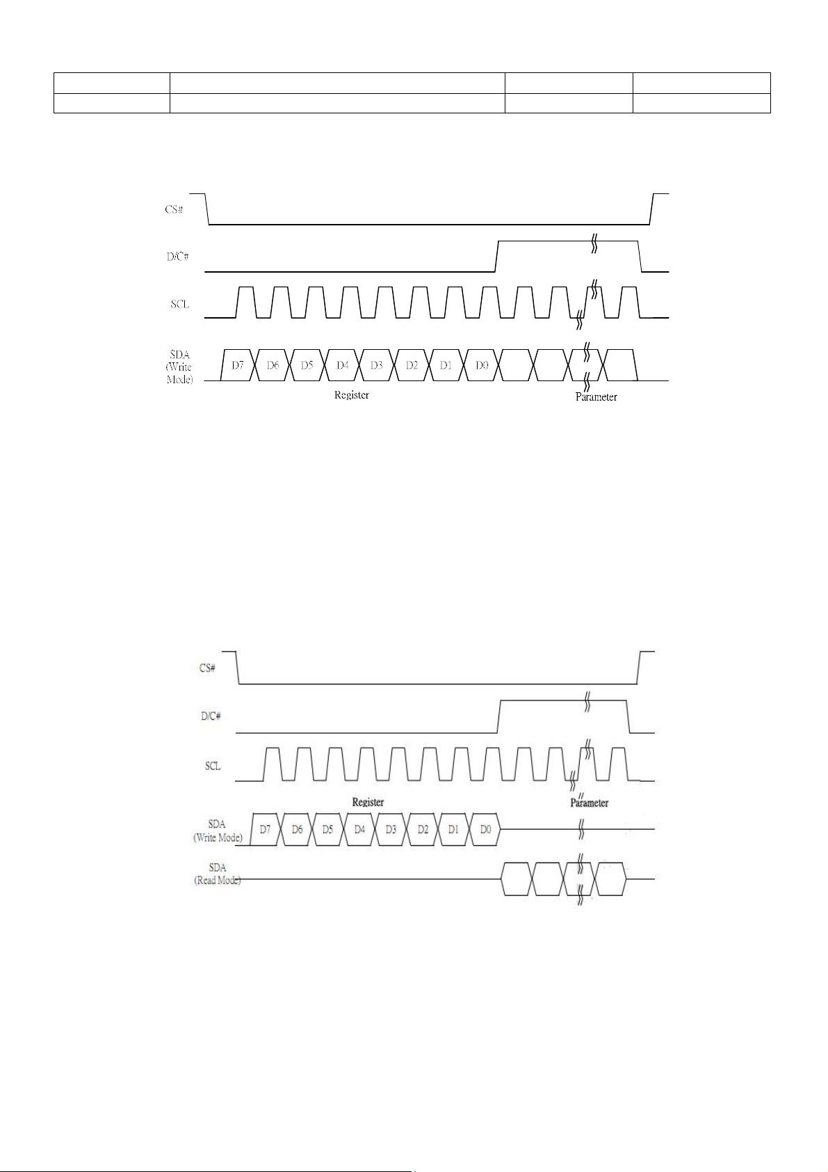
In the write mode, SDA is shifted into an 8-bit shift register on each rising edge of SCL in the order of
D7, D6, ... D0. The level of D/C# should be kept over the whole byte. The data byte in the shift
register is written to the Graphic Display Data RAM (RAM)/Data Byte register or command Byte
register according to D/C# pin.
Figure 7-1: Write procedure in 4-wire SPI mode
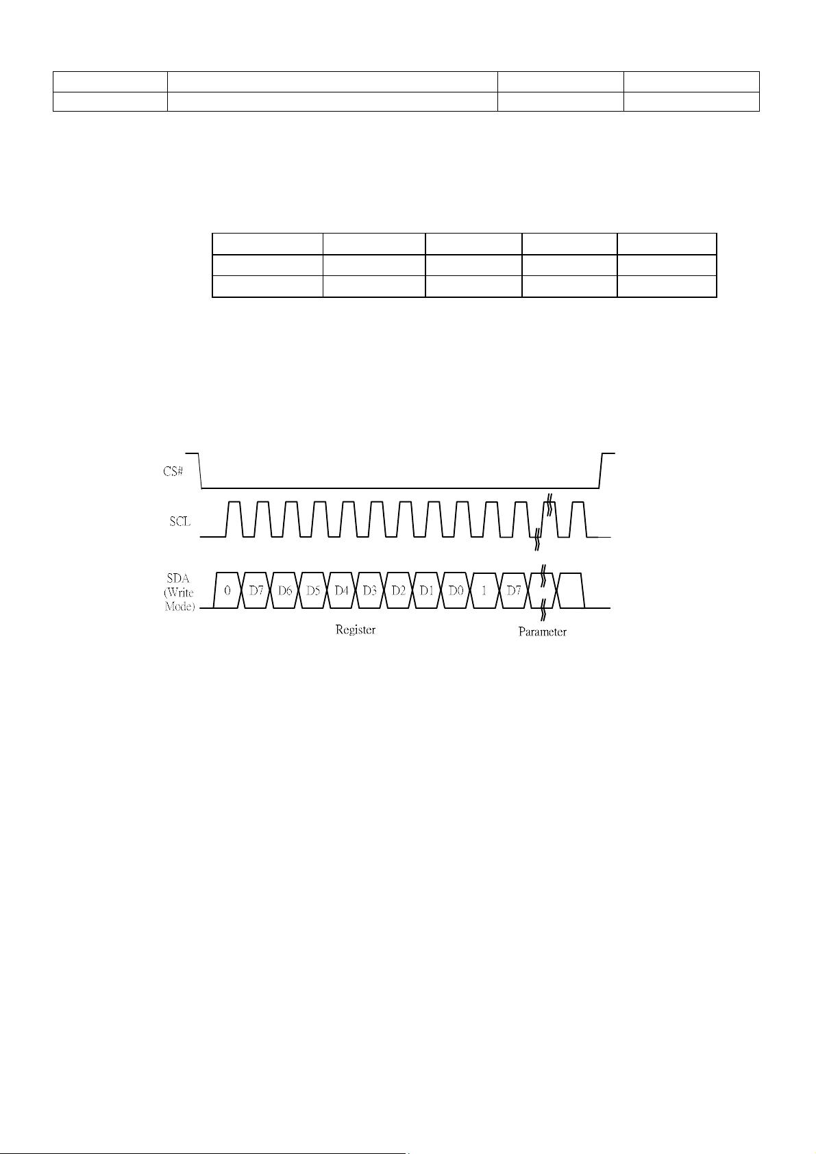
In the Read mode:
1. After driving CS# to low, MCU need to define the register to be read.
2. SDA is shifted into an 8-bit shift register on each rising edge of SCL in the order of D7, D6, ...
D0 with D/C# keep low.
3. After SCL change to low for the last bit of register, D/C# need to drive to high.
4. SDA is shifted out an 8-bit data on each falling edge of SCL in the order of D7, D6, … D0.
5. Depending on register type, more than 1 byte can be read out. After all byte are read, CS# need
to drive to high to stop the read operation.
Figure 7-2: Read procedure in 4-wire SPI mode
剩余41页未读,继续阅读


