
Data Sheet 7 Rev. 1.1
2018-03-07
TLF50281ELV50
2.2 MHz Step-Down Regulator 500 mA, 5 V, low quiescent current
General product characteristics
4 General product characteristics
4.1 Absolute maximum ratings
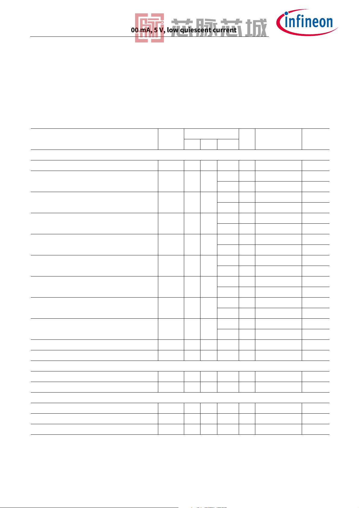
Table 1 Absolute maximum ratings
1)
T
j
= -40°C to 150°C; all voltages with respect to ground (unless otherwise specified)
1) Not subject to production test, specified by design
Parameter Symbol Values Unit Note or
Test Condition
Number
Min. Typ. Max.
Voltages
Enable input
V
EN
-40 – 45 V – P_4.1.1
Synchronization input
V
SYNC
-0.3 – 5.5 V – P_4.1.2
6.2 V
t
< 10 s
2)
2) ESD susceptibility HBM according to ANSI/ESDA/JEDEC JS-001.
P_4.1.3
Frequency adjustment pin
V
FREQ
-0.3 – 5.5 V – P_4.1.4
6.2 V
t
< 10 s
2)
P_4.1.5
Watchdog input
V
WI
-0.3 – 5.5 V – P_4.1.6
6.2 V
t
< 10 s
2)
P_4.1.7
Watchdog output
V
WO
-0.3 – 5.5 V – P_4.1.8
6.2 V
t
< 10 s
2)
P_4.1.9
Watchdog mode selection pin
V
WMSEL
-0.3 – 5.5 V – P_4.1.10
6.2 V
t
< 10 s
2)
P_4.1.11
Reset threshold adjust pin
V
RTADJ
-0.3 – 5.5 V – P_4.1.12
6.2 V
t
< 10 s
2)
P_4.1.13
Reset output
V
RO
-0.3 – 5.5 V – P_4.1.14
6.2 V
t
< 10 s
2)
P_4.1.15
Feedback Input
V
FB
-0.3 – 5.5 V – P_4.1.16
6.2 V
t
< 10 s
2)
P_4.1.17
Buck switch output
V
SWO
-2.0 –
V
VS + 0.3
V– P_4.1.18
Supply voltage input
V
VS
-0.3 – 45 V – P_4.1.19
Temperatures
Junction temperature
T
j
-40 – 150 °C – P_4.1.20
Storage temperature
T
stg
-55 – 150 °C – P_4.1.21
ESD susceptibility
ESD resistivity
V
ESD
-2 – 2 kV HBM P_4.1.22
ESD resistivity to GND
V
ESD
-500 – 500 V CDM
3)
3) ESD susceptibility, Charged Device Model “CDM” EIA/JESD22-C101 or ESDA STM5.3.1
P_4.1.23
ESD resistivity corner pins to GND
V
ESD
-750 – 750 V CDM
3)
P_4.1.24
剩余34页未读,继续阅读

芯脉芯城
- 粉丝: 3
- 资源: 4030
 我的内容管理
收起
我的内容管理
收起
- 我的资源
快来上传第一个资源
 我的收益 登录查看自己的收益
 我的积分
登录查看自己的积分
我的积分
登录查看自己的积分
 我的C币
登录后查看C币余额
我的C币
登录后查看C币余额
 我的收藏
我的收藏  我的下载
我的下载  下载帮助
下载帮助

会员权益专享


最新资源
- 构建智慧路灯大数据平台:物联网与节能解决方案
- 智慧开发区建设:探索创新解决方案
- SQL查询实践:员工、商品与销售数据分析
- 2022智慧酒店解决方案:提升服务效率与体验
- 2022年智慧景区信息化整体解决方案:打造数字化旅游新时代
- 2022智慧景区建设:大数据驱动的5A级管理与服务升级
- 2022智慧教育综合方案:迈向2.0时代的创新路径与实施策略
- 2022智慧教育:构建区域教育云,赋能学习新时代
- 2022智慧教室解决方案:融合技术提升教学新时代
- 构建智慧机场:2022年全面信息化解决方案
- 2022智慧机场建设:大数据与物联网引领的生态转型与客户体验升级
- 智慧机场2022安防解决方案:打造高效指挥与全面监控系统
- 2022智慧化工园区一体化管理与运营解决方案
- 2022智慧河长管理系统:科技助力水环境治理
- 伪随机相位编码雷达仿真及FFT增益分析
- 2022智慧管廊建设:工业化与智能化解决方案
资源上传下载、课程学习等过程中有任何疑问或建议,欢迎提出宝贵意见哦~我们会及时处理!
点击此处反馈


