LIU et al.: 0.55-V, 28-ppm/
◦
C, 83-nW CMOS SUB-BGR WITH ULTRALOW POWER CURVATURE COMPENSATION 97
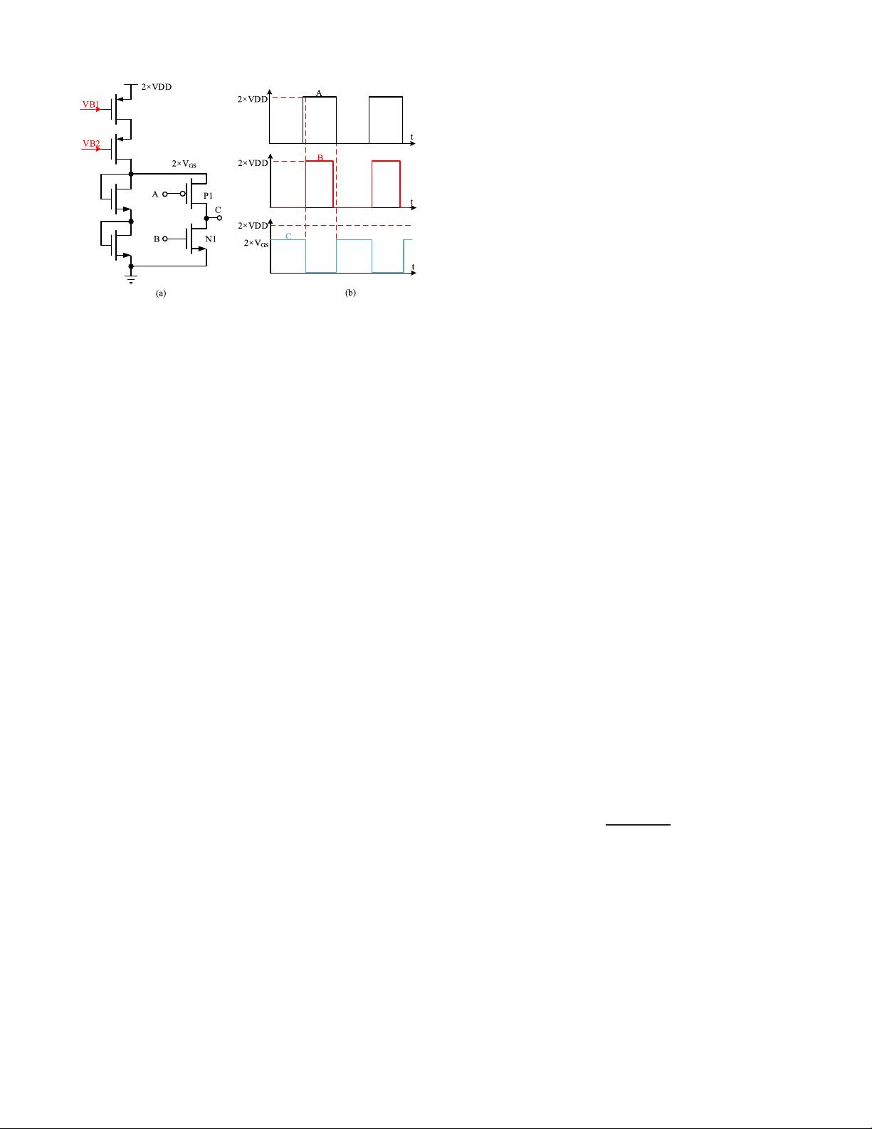
Fig. 4. (a) Clock scaling down circuit. (b) The control signal of the clock
scaling down circuit.
component. In our design, V
HOLD
is K×V
BE
, and it is between
120 mV and 240 mV under temperature variations. Thus, the
modified switch has a 50% lower leakage current compared
with the previous low leakage current switch at 120 °C.
Additionally, the error on the output of the divider, caused
by the leakage current, is reduced by 50%.
Another effect is the clock feedthrough and charge injection,
which only cause a constant error if the clock amplitude is
constant. However, when the supply voltage fluctuates, this
error is no longer constant and will deteriorate the precision
of K×V
BE
, resulting in poor line sensitivity (LS). In previ-
ous work [16], this effect was minimized by using dummy
MOSFETs, but this solution suffers from transistor mis-
match. In this paper, we solve this problem by restricting
the clock amplitude. Fig. 4 (a) shows the clock scaling down
circuit, and Fig. 4 (b) shows the control signal. We use 2×V
GS
as the supply voltage of the control signal in the switches.
As a result, when the supply voltage fluctuates, the clock
feedthrough and charge injection only cause a constant error.
Since the driving capability of 2×V
GS
is weak, clocks A and B
are not in phase, which prevents the pulse current from 2×V
GS
to GND.
The SC V
BE
divider with improved switches and the time
sequence of the control signals are shown in Fig. 5. The low
voltage oscillator provides a clock of 200 KHz for the control
signals. To reduce the power consumption of the SC divider, a
16-frequency-divider is used to reduce the operation frequency.
The R-C delay network and logic circuit are used to generate
the multi-phase control signals. The clock bootstrap [27] can
boost the amplitude of the control signal to 2×VDD.
There are 3 phases for the SC V
BE
divider. In the first
phase, switches S1 and S3 are on, and V
BE
is sampled
by C1. In the second phase, only switch S2 is on, and
C1 and C2 generate K(=C1/(C1+C2))×V
BE
. In the third
phase, switches S2 and S4 are on. In this phase, C1 and C2
work as a voltage source to charge C3. After several cycles,
the voltage across C3 is equal to K×V
BE
. The clock signals A
and A
dum
,BandB
dum
,CandC
dum
are two-phase non-overlap
clocks. As long as the switches are off, the amplifier’s output is
connected to the source or drain to reduce the leakage current.
A single stage amplifier with a PMOS input pair is used in the
divider, and the current consumption is approximately 2.5 nA.
C. Trimmable PTAT Voltage Generator
The SC V
BE
divider generates a high precision K×V
BE
.
This K×V
BE
should be added to the PTAT voltage to generate
a reference voltage. In this paper, to generate the PTAT
voltage, we use the circuit from [28]. This PTAT voltage is
generated by using the offset of an amplifier to avoid a large
resistor. By setting the input pair or the current mirror in the
amplifier to be different, the PTAT voltage is generated at
the two inputs of the amplifier. To compensate for K×V
BE
,
a 3-stage PTAT voltage generator is used, as shown in Fig. 6.
Therefore, the output reference voltage is
V
REF_NC
= K × V
BE
+ η × V
T
× ln(k
1
× k
2
× k
3
)
= K × V
BE
+ η × V
T
× ln
(
k
A
)
(3)
where k
1
is the width ratio of P8 and P7, k
2
is the width
ratio of P10 and P9, k
3
is width ratio of P12 and P11, and
k
A
= k
1
×k
2
×k
3
.TheV
REF_NC
has a large TC due to the lack
of curvature compensation. Thus, it is not suitable for high
precision applications. Figure 7 shows the simulation result
for voltage, V
REF_NC
, versus temperature. V
REF_NC
varies by
approximately 3.5 mV at a temperature range of −45 °C to
120 °C and its calculated TC is approximately 48 ppm/°C.
The accuracy of K×V
BE
across the process variations is
relatively high. However, there is an error that mainly comes
from the offset voltage in the PTAT generator because the
V
TH
mismatch is large. As shown in Fig. 6, a 3-bit trimming
circuit with a 3.25 mV average step was adopted to improve
the precision of the PTAT voltage. The 3-bit trimming is
realized by controlling the transistors, PM
T0
− PM
T2
,which
can change coefficients k
1
to k
3
in (3). In this design example,
the default trimming code is 100 for generating 461 mV of
reference voltage. Fig. 7 also shows the reference voltage when
the trimming code varies from 000 to 111. The trimming step
is not constant because the reference voltage is non-linear
under the control of k
1
− k
3
. However, the variation in the
trimming step can be reduced by choosing a proper transistor
size.
To improve the line sensitivity of the reference, the bias
current should also have low line sensitivity. Fig. 8 shows the
low voltage current source and the current mirror [27]. All of
the transistors work in the subthreshold region, and the current
flowing through resistor R
CS
is a PTAT current as
I
CS
=
V
T
× ln(n)
R
CS
(4)
where n is the size ratio of PM1 and PM2. A low voltage
amplifier consisting of PM3, PM4, NM3 and NM4 is used
to clamp the drain voltage of NM1 and NM2. It can reduce
the influence of the channel length modulation in NM1 and
NM2, and improve the line sensitivity of the current source.
The current mirror, which is powered by 2×VDD, is used to
generate the global bias voltages, VB1 and VB2, for the entire
circuit.
III. L
OW POWER CURVATURE COMPENSATION
A. Proposed Low Power Curvature Compensation
In recent years, several low power voltage references have
been published [6]–[10], [27], [28]. These voltage references


