硅光子学微结构:新型光学涡旋与超窄带近红外完美吸收应用探索
134 浏览量
更新于2024-08-27
收藏 3.24MB PDF 举报
"该研究深入探讨了一种新颖的硅光子学微结构,这些微结构支持光学涡旋和波导,以实现超窄带近红外光的完美吸收。通过设计硅光子学超材料,研究人员旨在优化近红外光的吸收性能,对相关物理机制进行了深入的理论与实验研究。"
在硅光子学领域,本文提出了一种创新的设计理念,即利用特殊构造的微结构来实现对近红外光的近乎完美的吸收。这一技术基于硅光子学超材料,这是一种具有独特光学特性的材料,能够对特定波长的光进行高效操控。研究的核心在于对不同物理机制的深入分析,这些机制是实现约100%的超窄带近红外光吸收的关键。
光学涡旋是一种具有螺旋相位的光束,其光场携带轨道角动量,这使得它们在信息传输、量子光学以及光与物质相互作用等领域有广泛应用。结合波导技术,这些微结构可以引导并控制光在纳米尺度上的传播,从而优化吸收效率。在硅基平台上实现这样的光子学设计,不仅能够提高光吸收的效率,还可能降低系统尺寸和功耗,这对于集成光电子设备来说尤其重要。
研究团队来自以色列的多个学术机构,包括Ben-Gurion大学的电气和计算机工程学院、Shamoon College of Engineering的电子与电气工程系、Jerusalem College of Technology的电气工程学院以及Ilse Katz Institute for Nanoscale Science & Technology。他们的工作经过了多次修订和完善,最终在2020年发表,为硅光子学领域开辟了新的研究方向。
文章详细描述了设计和实验过程,包括微结构的几何参数优化、光吸收的理论计算以及实验验证。通过对不同参数的调整,研究者探索了如何最大化近红外光的吸收,同时保持超窄的吸收带宽。这些发现对于提升光探测器、太阳能电池和光通信系统的性能有着重大意义。
这项研究深入剖析了新型硅光子学微结构的设计与应用,特别是在近红外光的高效吸收方面,这将对未来的光电子技术和光子学器件设计产生深远影响。通过理解并利用这些微结构背后的物理原理,科研人员有望开发出更先进、更高效的光子集成系统,推动信息技术的持续进步。
front air–Si
3
N
4
∕Si
3
N
4
with the back SiO
2
−Si
3
N
4
∕Si
3
N
4
GL
encloses the cavity. As shown in Fig. 1, we consider the
through-substrate backside illumination (BSI) at normal inci-
dence. Benefiting from the absence of the backside electrical
contacts, BSI has the essential advantage of reducing the PD
pixel size without decreasing the amount of input light power
[26], which is desirable for on-chip applications.
In this paper, we adopt the η A modeling, which simpli-
fies the design to one in which only the optics need to be con-
sidered. Herewith, rather than being restricted to a specific PD
technology, we analyze the structures optically, characterizing
the constitutive layers by complex RIs n ik, where n are
the real RIs and k ≪ n are the extinction coefficients. This
modeling still has widespread use for initial designs of the elec-
tronic PDs [16,18,21,22,26,27]. In such cases, optical model-
ing can be complemented and refined by an electron-device
simulation [18,28,29]; however, it is not expected to disprove
the optical modeling outcomes. The n and k spectra for the
involved materials are found in Refs. [30–32]; their values
at the CDW are given in Table 1.
Here, the design emphasis is put on obtaining the maximal
CDW efficiency η
max
max ηλ
0
, while maintaining t
a
con-
stant per design, and keeping the back-GL cladding’s thickness
(similarly to the DBR layers’ thicknesses) fixed at the quarter-
wave value t
qw
≈ 100.2nm. Such dimensions as Λ and the
groove width W (constrained for simplicity to be the same
for both GLs), etch depths t
fg
and t
bg
, as well as the thicknesses
of the front-grating cladding t
Si
3
N
4
and front and back cavities,
d
f
and d
b
, respectively, are the design variables. We observe the
SW regime, limiting ab initio the operation wavelengths from
below by the Rayleigh wavelength λ
R
Λn
SiO
2
, which sup-
presses the non-specular orders of the grating diffraction into
the cavity and so prevents losses due to light escaping from the
structure’s sides. Note that this is not compulsory since the
non-specular orders can be suppressed with extra constraints;
see, e.g., Refs. [21,33].
3. DESIGN PROCEDURE, OPTIMAL
STRUCTURES, AND THEIR EFFICIENCY
SPECTRA
We perform the computer-aided designs with an in-house soft-
ware run in MATLAB environment. The software consists of
two modules: “Simulation,” which contains the codes of an in-
house recast rigorous coupled-wave analysis (RCWA) for sim-
ulations of the structures merging smooth and grating-pat-
terned layers as described in detail elsewhere (see Ref. [21] and
references therein); and “Optimization,” which calls a multi-
start optimization algorithm from MATLAB Optimization
Toolbox [34–36] and a graphical user interface (GUI), which
forces the modules to interact and thus drives the simulations
and designs as shown in Fig. 2.
In order that the optimization would not be blind, we are
guided by an approach to obtaining initial (start, trial) design
parameters that, in modern terms, are geometric-phase control
[20]. Homogenizing the gratings as described in Appendix A,
we first design the front and back GLs to be standalone and to
be highly and lowly reflective (subsections A and B), respec-
tively, at a normal CDW incidence from a semi-infinite
SiO
2
. In this way, we assess trial values Λ
, W
, t
fg
, t
bg
,
t
Si
3
N
4
for the GLs’ parameters shown in Fig. 1. With these,
our RCWA code returns the GLs’ reflection-amplitudes’ phases
φ
f
and φ
b
, the sum of which Φ gives a rough idea on the
geometric phase of an unloaded dual-GL cavity. Φ leads
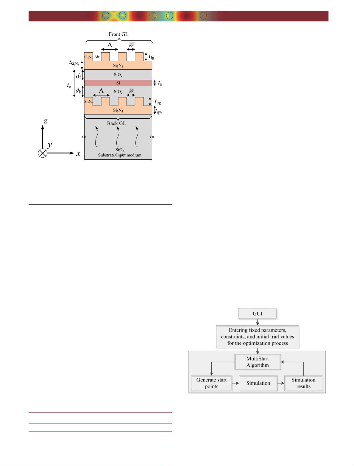
Fig. 1. Sketch of the enhanced light-absorption structure that com-
prises a cavity-embedding Si layer, two GLs enclosing the cavity, and a
substrate. The coordinate system is shown, where the grating perio-
dicity and grooves/lines are along the x and y axes, respectively,
and the layer stacking and light impinging directions are along the
z axis.
Table 1. RIs at the CDW of the Materials that Are Set in
the Text
λ
0
[μm] Si
3
N
4
SiO
2
Si
0.8 1.9962 i0 1.4533 i0 3.6925 i0.0065
Fig. 2. Sketchy flowchart of the optimization process. The GUI
Module inputs the trial parameters, assessed as described in the text,
fixed parameters, and constraints to the Optimization Module. There,
the trial-and-error multi-start algorithm generates the next start points
and inputs them into the Simulation Module, which feeds the algo-
rithm back and loops until attaining an optimum.
Research Article
Vol. 8, No. 3 / March 2020 / Photonics Research 383
剩余13页未读,继续阅读
2021-07-27 上传
2018-05-26 上传
2023-03-31 上传
2023-04-27 上传
2023-02-15 上传
2023-06-08 上传
2023-05-13 上传
2023-06-09 上传
2023-03-28 上传

weixin_38569219
- 粉丝: 4
- 资源: 984
 我的内容管理
展开
我的内容管理
展开


最新资源
- Google Test 1.8.x版本压缩包快速下载指南
- Java实现二叉搜索树的插入与查找功能
- Python库丰富性与数据可视化工具Matplotlib
- MATLAB通信仿真设计源代码与应用解析
- 响应式环保设备网站模板源码下载
- 微信小程序答疑平台完整设计源码案例
- 全元素DFT计算所需赝势UPF文件集合
- Object-C实现的Flutter组件开发详解
- 响应式环境设备网站模板下载 - 恒温恒湿机营销平台
- MATLAB绘图示例与知识点深入探讨
- DzzOffice平台新插件:excalidraw白板功能介绍与使用指南
- Java基础实训教程:电子商城项目开发与实践
- 物业集团管理系统数据库设计项目完整复刻包
- 三五族半导体能带参数计算器:精准模拟与应用
- 毕业论文:基于SSM框架的毕业生跟踪调查反馈系统设计与实现
- 国产化数据库适配:人大金仓与达梦实践教程
