
388
IEEE JOURNAL OF SOLID-STATECIRCUITS,VOL.SC-9,NO. 6, DECEMBER 1974
A Simple Three-Terminal IC Bandgap Reference
A. PAUL BROKAW, MEMBER, IEEE
A?r.sfrac
f—A new configuration for realization of a stabilized
bandgap voltage is described, The new two-transistor circuit uses
collector current sensing to eliminate errors due to base current.
Because the stabilized voltage appears at a high impedance point,
the application to circuits with higher output voltage is simplified.
Incorporation of the new two-transistor cell in a three-terminal
2.5-V monolithic reference is described. The complete circuit is
outlined in functional detail together with analytical methods used
in the design. The analytical results include sensitivity coefficients,
gain and frequency response parameters, and biasing for optimum
temperature performance. The performance of the monolithic cir-
cuit, which includes temperature coefficients of 5 ppm/ “C over the
military temperaturerange, is reported.
I. INTRODUCTION
T
HE REQUIREMENT for a stable reference volt-
age is almost universal in electronic design. The
temperature-compensatecl avalanche breakdown
diode fills many of the needs, but cannot be used with
low voltage supplies and often suffers from long-term
stability problems. Use of a transistor
base emitter diode
temperature compensated to the bandgap voltage of
silicon is a technique which overcomes some of the
avalanche cliode limitations. Bandgap circuits can be
operated from low voltage sources and depend mainly
upon subsurface effects which tend to be more stable
than the surface breakdowns generally obtained with
avalanche diodes.
The conventional three-transistor bandgap cell works
well for very low voltage two-terminal or ‘synthetic
Zener cliocle” requirements. The tlmee-transistor cell is
less flexible in three-terminal applications and in cir-
cuits where the desired output is not an integral multiple
of the bandgap voltage.
The two-transistor cell presented here is simpler,
more flexible in three-terminal applications, and elim-
inates sources of error inherent in the three-transistor
cell. The
two-transistor cell offers separate control over
output voltage and temperature coefficient in a circuit
using only a single control loop.
The new bandgap circuit has been used as the basis
of a monolithic three-terminal reference circuit sup-
plying
a stable 2.5-V output and operating down to
4-V input.
11,
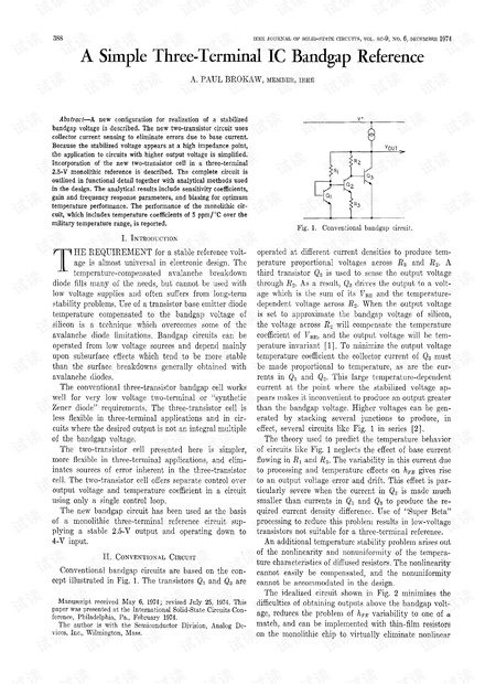
CONVENTIONAL CIRCUIT
Conventional bandgap circuits are based on the con-
cept illustrated in Fig. 1. The transistors QI and Qz are
Manuscript received May 6, 1974; revised July 25, 1974. This
p~per was presented at the International Solid-State Circuits Con-
ference, Philadelphia, Pa., February 1974.
The author is with the Semiconductor Division, Analog De-
vices, Inc., Wilmington, Mass.
v+
,
--f--Q%
1
~
!
Fig. 1. Conventional bandgap circuit.
operated at different current densities to produce tem-
perature proportional voltages across R~ and Rz. A
third transistor Q3 is used to sense the output voltage
through Rz. As a result, Q8 drives the output to a volt-
age which is the sum of its ~7~E and the tcmperature-
dependent voltage across Rz. When the output voltage
is set to approximate the banclgap voltage of silicon,
the voltage across Rz will compensate the temperature
coefficient of VBE, and the output voltage will be tem-
perature invariant [1]. To minimize the output voltage
temperature coefficient the collector current of Qa must
be made proportional to temperature, as are the cur-
rents in QI and Qz. This large temperature-clependent
current at the point where the stabilized voltage ap-
pears makes it inconvenient to produce an output greater
than the bandgap voltage. Higher voltages can be gen-
erated by stacking several junctions to produce, in
effect, several circuits like Fig. 1 in series [2].
The theory used to predict the temperature behavior
of circuits like Fig. 1 neglects the effect of base current
flowing in RI and R,. The
variability in this current due
to processing and temperature effects on hrn gives rise
to an output voltage error and drift. This effect is par-
ticularly severe when the current in Q2 is made much
smaller than currents in Q1 and Q8 to produce the re-
quired current density difference. Use of “Super Beta”
processing to reduce this problem results in low-voltage
transistors not suitable for a three-terminal reference.
An additional temperature stability problem arises out
of the nonlinearity and nonuniformity of the tempera-
ture characteristics of diffused resistors. The nonlinearity
cannot easily be compensatecl, ancl the nonuniformity
cannot be accommodated in the design.
The idealized circuit shown in Fig. 2 minimizes the
difficulties of obtaining outputs above the bandgap volt-
age, reduces the problem
of hj,E variability to one of ~
match, and can be implemented with thin-film resistors
on the monolithic chip to virtually eliminate nonlinear

L夫
- 粉丝: 0
- 资源: 1
 我的内容管理
收起
我的内容管理
收起
- 我的资源
快来上传第一个资源
 我的收益 登录查看自己的收益
 我的积分
登录查看自己的积分
我的积分
登录查看自己的积分
 我的C币
登录后查看C币余额
我的C币
登录后查看C币余额
 我的收藏
我的收藏  我的下载
我的下载  下载帮助
下载帮助

会员权益专享


最新资源
- zigbee-cluster-library-specification
- JSBSim Reference Manual
- c++校园超市商品信息管理系统课程设计说明书(含源代码) (2).pdf
- 建筑供配电系统相关课件.pptx
- 企业管理规章制度及管理模式.doc
- vb打开摄像头.doc
- 云计算-可信计算中认证协议改进方案.pdf
- [详细完整版]单片机编程4.ppt
- c语言常用算法.pdf
- c++经典程序代码大全.pdf
- 单片机数字时钟资料.doc
- 11项目管理前沿1.0.pptx
- 基于ssm的“魅力”繁峙宣传网站的设计与实现论文.doc
- 智慧交通综合解决方案.pptx
- 建筑防潮设计-PowerPointPresentati.pptx
- SPC统计过程控制程序.pptx
资源上传下载、课程学习等过程中有任何疑问或建议,欢迎提出宝贵意见哦~我们会及时处理!
点击此处反馈


评论0