DFI DDR PHY接口3.1规范更新:支持DDR3与LPDDR2
DFI (Design for Interconnectivity) DDR PHY (Phase-Locked Loop Dynamic Random Access Memory Physical Layer) Interface Specification v3.1 是一个详细的规范,旨在定义和管理DDR (Double Data Rate)内存接口的标准,特别是在DDR3和LPDDR2技术的实现中。这个版本是在2014年3月21日发布的,由Cadence Design Systems, Inc. 负责制定。
该规范的3.1版经历了多个关键更新和改进阶段:
1. 初始版本1.0在2007年1月30日发布,主要为DDR3支持奠定了基础。
2. 在2007年7月17日的2.0版本中,对DDR3支持进行了扩展,包括添加了读写级别控制功能。
3. 11月21日的2.0版本进一步优化,移除了关于PHY评估模式的数据眼睛训练相关内容,并引入了专门的门级训练模式信号,同时改进了读训练的术语表述和图例标准化。
4. 2008年3月26日的2.0版本加入了新的时序参数trdlvl_en和twrlvl_en,以及信号dfi_rdlvl_edge,增强了接口的灵活性和性能。
2008年10月2日的2.1版本增加了对初始LPDDR2的支持,并修正了2.0版中的小错误。
最后,在2008年11月24日的2.1版本中,规范引入了频率变化协议,对信号时序定义进行了详尽说明,还新增了trdlvl_load和twrlvl_...(此处省略了一些可能的细节)。
这些改动反映了随着内存技术的发展,DFI DDR PHY Interface标准不断适应新需求,确保了芯片设计者能够高效地与DDR和LPDDR2内存进行无缝通信。理解并遵循这一规范对于开发兼容高性能DDR内存系统的硬件和软件至关重要,它涵盖了物理层的详细操作规则、信号交互以及性能优化策略。
Architecture
16 of 141 DDR PHY Interface, Version 3.1
Copyright 1995-2014 March 21, 2014
Cadence Design Systems, Inc.
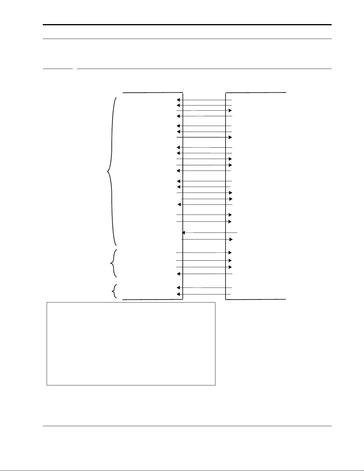
FIGURE 1. Block Diagram of Interface Signals: Control, Write, Read, Update and Status
dfi_wrdata_en
1
_pN
2
dfi_we_n
_3
_pN
2
dfi_reset_n
11
_pN
2
dfi_wrdata
1
_pN
2
dfi_wrdata_mask
1, 7
_pN
2
Write Data
Interface
dfi_rddata_en
1
_pN
2
Read Data
Interface
dfi_address
1
_pN
2
dfi_bank
3
_pN
2
dfi_ras_n
3
_pN
2
dfi_cke
1
_pN
2
dfi_cs_n
1
_pN
2
dfi_odt
5
_pN
2
Control
Interface
dfi_cas_n
3
_pN
2
dfi_act_n
4
_pN
2
dfi_bg
4
_pN
2
dfi_cid
4
_pN
2
dfi_wrdata_cs_n
1
__pN
2
dfi_rddata
1
_wN
2
dfi_rddata_valid
1
_wN
2
dfi_dram_clk_disable
1
dfi_init_start
1
dfi_data_byte_disable
1
Status
Interface
dfi_phyupd_req
1
dfi_ctrlupd_req
1
dfi_ctrlupd_ack
1
dfi_phyupd_type
1
dfi_phyupd_ack
1
Update
Interface
dfi_parity_in
1
_pN
2
dfi_alert_n_aN
1
dfi_freq_ratio
2
dfi_init_complete
1
MC
1. Used by all DRAMs.
2. Optional suffix for frequency ratio systems.
3. Used with DDR4, DDR3, DDR2, DDR1 and LPDDR1 DRAMs.
4. Used with DDR4 DRAM only.
5. Used with DDR4, DDR3, DDR2 and LPDDR3 DRAMs.
6. Used with LPDDR2 DRAM only.
7. Dual-function signal. In DDR4 systems with write DBI enabled, the
signal transforms from a mask to a write DBI signal.
8. Used with DDR4, DDR3, LPDDR3 and LPDDR2 DRAMs.
9. Used with DDR4, DDR3 and LPDDR3 DRAMs.
10. Used with LPDDR3 DRAMs only.
11. Used with DDR4 and DDR3 DRAMs.
Italicized text indicates that the phase/word/cycle is optional.
PHY
dfi_rddata_dbi_n
4
_wN
2
dfi_rddata_dnv
6
_wN
2
dfi_rddata_cs_n
1
_pN
2

剩余140页未读,继续阅读
1063 浏览量
338 浏览量
2812 浏览量
142 浏览量
142 浏览量
646 浏览量
点击了解资源详情
点击了解资源详情
点击了解资源详情


