
60
65
70
75
80
85
90
95
100
105
110
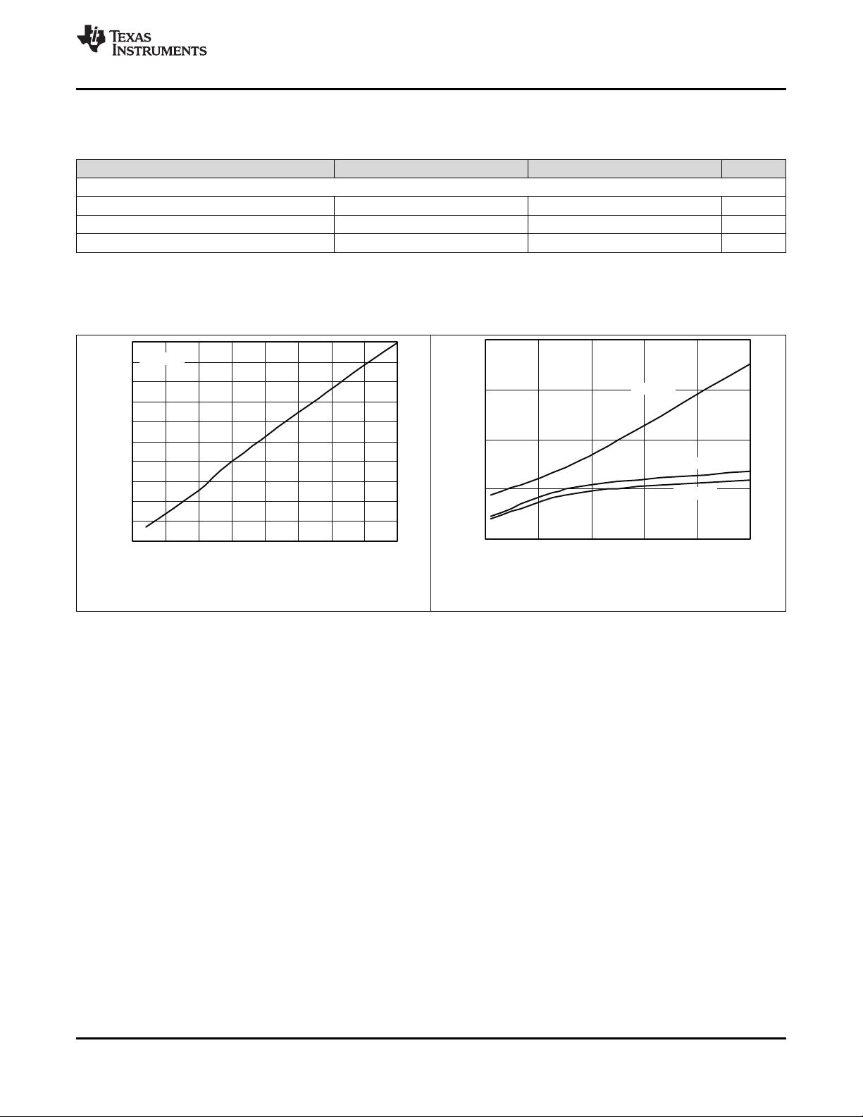
-50 -25 0 25 50 75 100 125 150
T -JunctionTemperature-°C
J
Rdson-OnResistance-mW
VIN=12V
0
1
2
3
4
3 8 13 18 23 28
V -InputVoltage-V
I
Isd-ShutdownCurrent- Am
EN=0V
T =150°C
J
T =25°C
J
T =-40°C
J
TPS54331
www.ti.com
SLVS839F –JULY 2008–REVISED OCTOBER 2014
7.6 Switching Characteristics
T
J
= –40°C to 150°C, VIN = 3.5 to 28 V (unless otherwise noted)
PARAMETER TEST CONDITIONS MIN TYP MAX UNIT
SWITCHING FREQUENCY
Switching Frequency VIN = 12 V, 25°C 456 570 684 kHz
Minimum controllable on time VIN = 12 V, 25°C 105 130 ns
Maximum controllable duty ratio
(1)
BOOT-PH = 6 V 90% 93%
(1) Specified by design
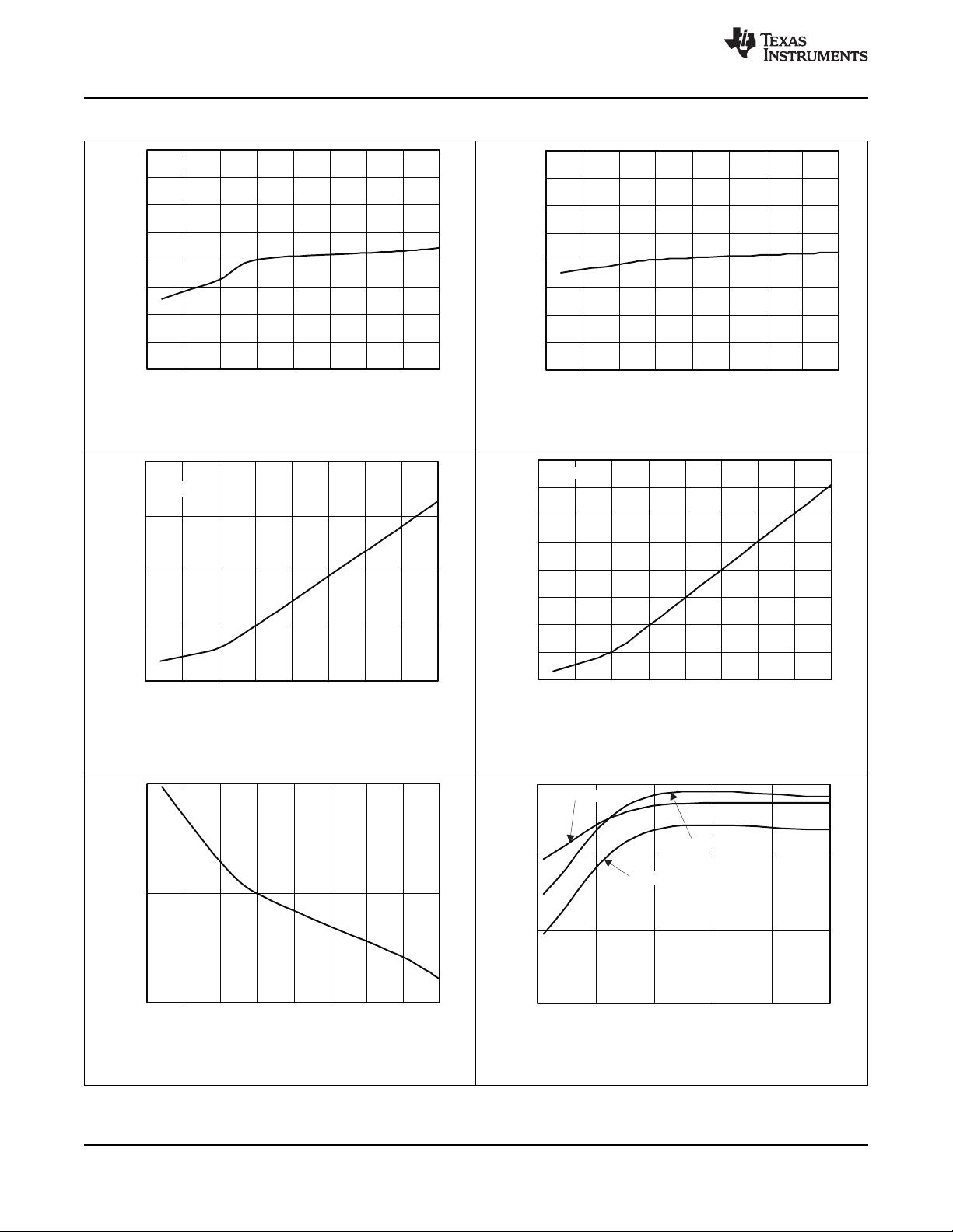
7.7 Typical Characteristics
Figure 2. Shutdown Quiescent Current vs Input Voltage
Figure 1. ON Resistance vs Junction Temperature
Copyright © 2008–2014, Texas Instruments Incorporated Submit Documentation Feedback 7
Product Folder Links: TPS54331
剩余35页未读,继续阅读


