
Everest Semiconductor Confidential ES8316
Revision 6.0 3 September 2018
Latest datasheet: www.everest-semi.com
or info@everest-semi.com
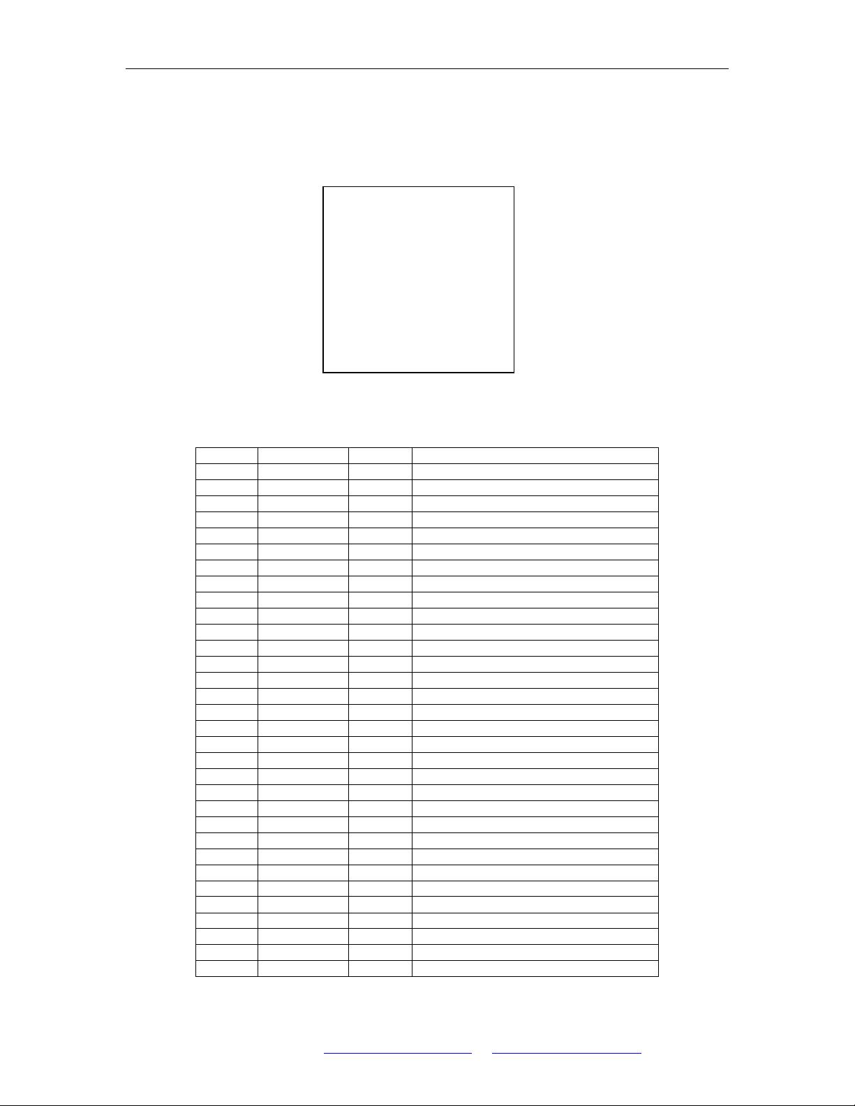
2. PIN OUT AND DESCRIPTION
PIN
NAME
I/O
DESCRIPTION
1 CCLK I I
2
C clock input
2 MCLK I Master clock
3 DVDD Supply Digital core supply
4
PVDD
Supply
Digital IO supply
5 DGND Supply Digital ground
6
SCLK
I/O
Audio data bit clock
7 DSDIN I DAC audio data
8
DLRCK
I/O
DAC audio data left and right clock
9 ASDOUT O ADC audio data
10
GPIO1
I/O
General purpose IO
11 GPIO2 I/O General purpose IO
12
GPIO3
I/O
General purpose IO
13 CPVSSP Charge pump filtering
14
CPVDD
Charge pump power supply
15 CPTOP Charge pump capacitor top
16
CPBOT
Charge pump capacitor bottom
17 CPGND Charge pump ground
18
CPGNDREF
Charge pump filtering
19 ROUT O Right analog output
20
LOUT
O
Left analog output
21 DACVREF O Decoupling capacitor
22
AVDD
Supply
Analog supply
23 AGND Supply Analog ground
24
ADCVREF
O
Decoupling capacitor
25 VMID O Decoupling capacitor
26
MICBIAS
O
Mic bias
27 RIN2 I Right analog input
28
LIN2
I
Left analog input
29 RIN1 I Right analog input
30
LIN1
I
Left analog input
31 CE I I
2
C device address selection
32
CDATA
I/O
I
2
C data input or output
ES8316
CCLK
MCLK
DVDD
PVDD
DGND
SCLK
DSDIN
DLRCK
1
2
3
4
5
6
7
8
ADCVREF
AGND
AVDD
DACVREF
LOUT
ROUT
CPGNDREF
CPGND
24
23
22
21
20
19
18
17
VMID
MICBIAS
RIN2
LIN2
RIN1
LIN1
CE
CDATA
25
26
27
28
29
30
31
32
CPBOT
CPTOP
CPVDD
CPVSSP
GPIO3
GPIO2
GPIO1
ASDOUT
16
15
14
13
12
11
10
9
剩余11页未读,继续阅读

qianxuncsu
- 粉丝: 6
- 资源: 37
 我的内容管理
收起
我的内容管理
收起
- 我的资源
快来上传第一个资源
 我的收益 登录查看自己的收益
 我的积分
登录查看自己的积分
我的积分
登录查看自己的积分
 我的C币
登录后查看C币余额
我的C币
登录后查看C币余额
 我的收藏
我的收藏  我的下载
我的下载  下载帮助
下载帮助

会员权益专享


最新资源
- 利用迪杰斯特拉算法的全国交通咨询系统设计与实现
- 全国交通咨询系统C++实现源码解析
- DFT与FFT应用:信号频谱分析实验
- MATLAB图论算法实现:最小费用最大流
- MATLAB常用命令完全指南
- 共创智慧灯杆数据运营公司——抢占5G市场
- 中山农情统计分析系统项目实施与管理策略
- XX省中小学智慧校园建设实施方案
- 中山农情统计分析系统项目实施方案
- MATLAB函数详解:从Text到Size的实用指南
- 考虑速度与加速度限制的工业机器人轨迹规划与实时补偿算法
- Matlab进行统计回归分析:从单因素到双因素方差分析
- 智慧灯杆数据运营公司策划书:抢占5G市场,打造智慧城市新载体
- Photoshop基础与色彩知识:信息时代的PS认证考试全攻略
- Photoshop技能测试:核心概念与操作
- Photoshop试题与答案详解
资源上传下载、课程学习等过程中有任何疑问或建议,欢迎提出宝贵意见哦~我们会及时处理!
点击此处反馈


