没有合适的资源?快使用搜索试试~ 我知道了~
首页BlueNRG开发手册
BlueNRG开发手册
需积分: 49 328 浏览量
更新于2023-05-20
评论 1
收藏 5.46MB PDF 举报
Bluetooth specification compliant master, slave and multiple roles simultaneously, single-mode Bluetooth low energy systemon-chip
资源详情
资源评论
资源推荐

June 2016
DocID028866 Rev 1
1/173
This is information on a product in full production.
www.st.com
BlueNRG-1
Bluetooth
®
low energy wireless system-on-chip
Datasheet - production data
Features
Bluetooth specification compliant master,
slave and multiple roles simultaneously,
single-mode Bluetooth low energy system-
on-chip
Operating supply voltage: from 1.7 to 3.6 V
Integrated linear regulator and DC-DC step-
down converter
Operating temperature range: -40 °C to 105
°C
High performance, ultra-low power Cortex-
M0 32-bit based architecture core
Programmable 160 KB Flash
24 KB RAM with retention (two 12 KB
banks)
1 x UART interface
1 x SPI interface
2 x I
2
C interface
14 or 15 GPIO
2 x multifunction timer
10-bit ADC
Watchdog & RTC
DMA controller
PDM stream processor
16 or 32 MHz crystal oscillator
32 kHz crystal oscillator
32 kHz ring oscillator
Battery voltage monitor and temperature
sensor
Up to +8 dBm available output power (at
antenna connector)
Excellent RF link budget (up to 96 dB)
Accurate RSSI to allow power control
8.2 mA maximum TX current (@ 0 dBm, 3.0
V)
Down to 1 µA current consumption with
active BLE stack (sleep mode)
Compliant with the following radio frequency
regulations: ETSI EN 300 328, EN 300 440,
FCC CFR47 Part 15, ARIB STD-T66
Pre-programmed bootloader via UART
QFN32, WCSP34 package option
Dedicated wettable flank QFN package for
automotive grade qualification
Applications
Automotive product
Watches
Fitness, wellness and sports
Consumer medical
Security/proximity
Remote control
Home and industrial automation
Assisted living
Mobile phone peripherals
Lighting
PC peripherals
Table 1: Device summary table
Order code
Package
Packing
BLUENRG-132
QFN32
(5 x 5 mm)
Tape and reel
BLUENRG-134
WLCSP34
Tape and reel
BLUENRG-132Y
QFN32
(5 x 5 mm)
Automotive
grade Level
Tape and reel
WLCSP34
QFN32

Contents
BlueNRG-1
2/173
DocID028866 Rev 1
Contents
1 Description..................................................................................... 11
2 BlueNRG-1 Bluetooth low energy stack ...................................... 12
3 Functional details .......................................................................... 14
3.1 Core ................................................................................................ 14
3.2 Interrupts ......................................................................................... 14
3.3 Memories ........................................................................................ 16
3.4 Power management ........................................................................ 16
3.4.1 States description ............................................................................. 16
3.4.2 Power saving strategy ...................................................................... 17
3.4.3 System controller registers ............................................................... 18
3.5 Clocks and reset management........................................................ 20
3.5.1 Reset management .......................................................................... 21
3.5.2 Reset and wakeup reason decoding ................................................ 22
3.5.3 Switching to external clock ............................................................... 22
3.5.4 Clock and reset registers .................................................................. 23
3.6 ADC ................................................................................................ 27
3.6.1 Introduction ....................................................................................... 27
3.6.2 Functional overview .......................................................................... 27
3.6.3 ADC registers ................................................................................... 30
3.7 DMA ................................................................................................ 34
3.7.1 Introduction ....................................................................................... 34
3.7.2 Functional overview .......................................................................... 34
3.7.3 DMA registers ................................................................................... 41
3.8 SPI .................................................................................................. 49
3.8.1 Introduction ....................................................................................... 49
3.8.2 Functional overview .......................................................................... 50
3.8.3 SPI registers ..................................................................................... 54
3.9 UART .............................................................................................. 61
3.9.1 Introduction ....................................................................................... 61
3.9.2 Functional description....................................................................... 61
3.9.3 UART registers ................................................................................. 69
3.10 I2C .................................................................................................. 82
3.10.1 Introduction ....................................................................................... 82
3.10.2 Functional description....................................................................... 82
3.10.3 I
2
C registers ...................................................................................... 84

BlueNRG-1
Contents
DocID028866 Rev 1
3/173
3.11 Flash controller .............................................................................. 101
3.11.1 Flash controller introduction ........................................................... 101
3.11.2 Flash controller functional description ............................................ 101
3.11.3 Flash controller registers ................................................................ 104
3.12 GPIO ............................................................................................. 108
3.12.1 Introduction ..................................................................................... 108
3.12.2 Functional description..................................................................... 108
3.12.3 GPIO registers ................................................................................ 111
3.13 MFT ............................................................................................... 116
3.13.1 MFT introduction ............................................................................. 116
3.13.2 MFT functional description ............................................................. 116
3.13.3 MFT registers ................................................................................. 126
3.14 Watchdog ...................................................................................... 128
3.14.1 Introduction ..................................................................................... 128
3.14.2 Functional description..................................................................... 129
3.14.3 Watchdog registers ......................................................................... 129
3.15 RTC ............................................................................................... 132
3.15.1 Introduction ..................................................................................... 132
3.15.2 Functional description..................................................................... 132
3.15.3 RTC registers ................................................................................. 134
3.16 RNG .............................................................................................. 141
3.16.1 Introduction ..................................................................................... 141
3.16.2 Functional description..................................................................... 141
3.16.3 RNG registers ................................................................................. 141
3.17 PDM stream processor ................................................................. 142
3.18 System timer (SysTick) ................................................................. 142
3.19 TX/RX event alert .......................................................................... 142
3.20 SWD debug feature ....................................................................... 143
3.20.1 Debugging tips ................................................................................ 143
3.21 Bluetooth low energy radio ............................................................ 143
3.21.1 Radio operating modes .................................................................. 143
3.22 Pre-programmed bootloader ......................................................... 144
4 Pin description ............................................................................ 145
5 Memory mapping ......................................................................... 149
6 Application circuit ....................................................................... 151
7 Absolute maximum ratings and thermal data ........................... 154

Contents
BlueNRG-1
4/173
DocID028866 Rev 1
8 General characteristics ............................................................... 155
9 Electrical specification ................................................................ 156
9.1 Electrical characteristics ................................................................ 156
9.1.1 Peripheral current consumption ..................................................... 157
9.2 RF general characteristics ............................................................ 157
9.3 RF transmitter characteristics ........................................................ 158
9.4 RF receiver characteristics ............................................................ 158
9.5 High speed crystal oscillator characteristics .................................. 160
9.5.1 High speed crystal oscillator ........................................................... 161
9.6 Low speed crystal oscillator characteristics .................................. 162
9.7 High speed ring oscillator characteristics ...................................... 162
9.8 Low speed ring oscillator characteristics ....................................... 162
9.9 N-fractional frequency synthesizer characteristics ........................ 162
9.10 Auxiliary blocks characteristics ...................................................... 163
10 Package information ................................................................... 165
10.1 QFN32 package information ......................................................... 166
10.2 WLCSP34 package information .................................................... 168
11 PCB assembly guidelines ........................................................... 170
12 Revision history .......................................................................... 172

BlueNRG-1
List of tables
DocID028866 Rev 1
5/173
List of tables
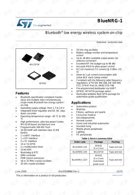
Table 1: Device summary table .................................................................................................................. 1
Table 2: Interrupt vectors .......................................................................................................................... 15
Table 3: Relationship between BlueNRG-1 states and functional blocks ................................................ 17
Table 4: SYSTEM_CTRL registers ........................................................................................................... 18
Table 5: SYSTEM_CTRL - WKP_IO_IS register description: address offset
SYSTEM_CTRL_BASE_ADDR+0x00 ...................................................................................................... 18
Table 6: SYSTEM_CTRL - WKP_IO_IE register description: address offset
SYSTEM_CTRL_BASE_ADDR+0x04 ...................................................................................................... 19
Table 7: SYSTEM_CTRL - CTRL register description: address offset
SYSTEM_CTRL_BASE_ADDR+0x08 ...................................................................................................... 19
Table 8: AHBUPCONV registers .............................................................................................................. 19
Table 9: BLUE_CTRL registers ................................................................................................................ 19
Table 10: CKGEN_SOC registers ............................................................................................................ 23
Table 11: CKGEN_SOC - CONTROL register description: address offset
CKGEN_SOC_BASE_ADDR+0x00 ......................................................................................................... 23
Table 12: CKGEN_SOC - REASON_RST register description: address offset
CKGEN_SOC_BASE_ADDR+0x08 ......................................................................................................... 24
Table 13: CKGEN_SOC - DIE_ID register description: address offset
CKGEN_SOC_BASE_ADDR+0x1C ......................................................................................................... 24
Table 14: CKGEN_SOC - CLOCK_EN register description: address offset
CKGEN_SOC_BASE_ADDR+0x20 ......................................................................................................... 24
Table 15: CKGEN_SOC - DMA_CONFIG register description: address offset
CKGEN_SOC_BASE_ADDR+0x24 ......................................................................................................... 25
Table 16: CKGEN_BLE registers ............................................................................................................. 25
Table 17: CKGEN_BLE - REASON_RST register description: address offset
CKGEN_BLE_BASE_ADDR+0x08 .......................................................................................................... 25
Table 18: CKGEN_BLE - CLK32K_COUNT register description: address offset
CKGEN_BLE_BASE_ADDR+0x0C .......................................................................................................... 26
Table 19: CKGEN_BLE - CLK32K_PERIOD register description: address offset
CKGEN_BLE_BASE_ADDR+0x10 .......................................................................................................... 26
Table 20: CKGEN_BLE - CLK32K_FREQ register description: address offset
CKGEN_BLE_BASE_ADDR+0x14 .......................................................................................................... 26
Table 21: CKGEN_BLE - CLK32K_IT register description: address offset
CKGEN_BLE_BASE_ADDR+0x18 .......................................................................................................... 26
Table 22: ADC channels ........................................................................................................................... 27
Table 23: ADC data rate ........................................................................................................................... 28
Table 24: ADC data rate with microphone mode ...................................................................................... 28
Table 25: ADC registers............................................................................................................................ 30
Table 26: ADC - CTRL register description: address offset ADC_BASE_ADDR+0x00 ........................... 30
Table 27: ADC - CONF register description: address offset ADC_BASE_ADDR+0x04 .......................... 31
Table 28: ADC - IRQSTAT register description: address offset ADC_BASE_ADDR+0x08..................... 32
Table 29: ADC - IRQMASK register description: address offset ADC_BASE_ADDR+0x0C ................... 33
Table 30: ADC - DATA_CONV register description: address offset ADC_BASE_ADDR+0x14 .............. 33
Table 31: ADC - OFFSET register description: address offset ADC_BASE_ADDR+0x18 ...................... 33
Table 32: ADC - SR_REG register description: address offset ADC_BASE_ADDR+0x20 ..................... 33
Table 33: ADC - THRESHOLD_HI register description: address offset ADC_BASE_ADDR+0x24 ........ 34
Table 34: ADC - THRESHOLD_LO register description: address offset ADC_BASE_ADDR+0x28 ....... 34
Table 35: Programmable data width and endian behavior (when bits PINC = MINC = 1) ....................... 37
Table 36: DMA interrupt requests ............................................................................................................. 40
Table 37: DMA registers ........................................................................................................................... 41
Table 38: DMA - ISR register description: address offset DMA_BASE_ADDR+0x00 ............................. 41
Table 39: DMA - IFCR register description: address offset DMA_BASE_ADDR+0x04 ........................... 45
Table 40: DMA_CHx registers .................................................................................................................. 47
剩余172页未读,继续阅读

安全验证
文档复制为VIP权益,开通VIP直接复制

评论0