
SLRS049C − FEBRUARY1997 − REVISED AUGUST 2004
1
POST OFFICE BOX 655303 • DALLAS, TEXAS 75265
D 500-mA Rated Collector Current (Single
Output)
D High-Voltage Outputs ...50 V
D Output Clamp Diodes
D Inputs Compatible With Various Types of
Logic
D Relay Driver Applications
D Compatible with ULN2800A Series
description/ordering information
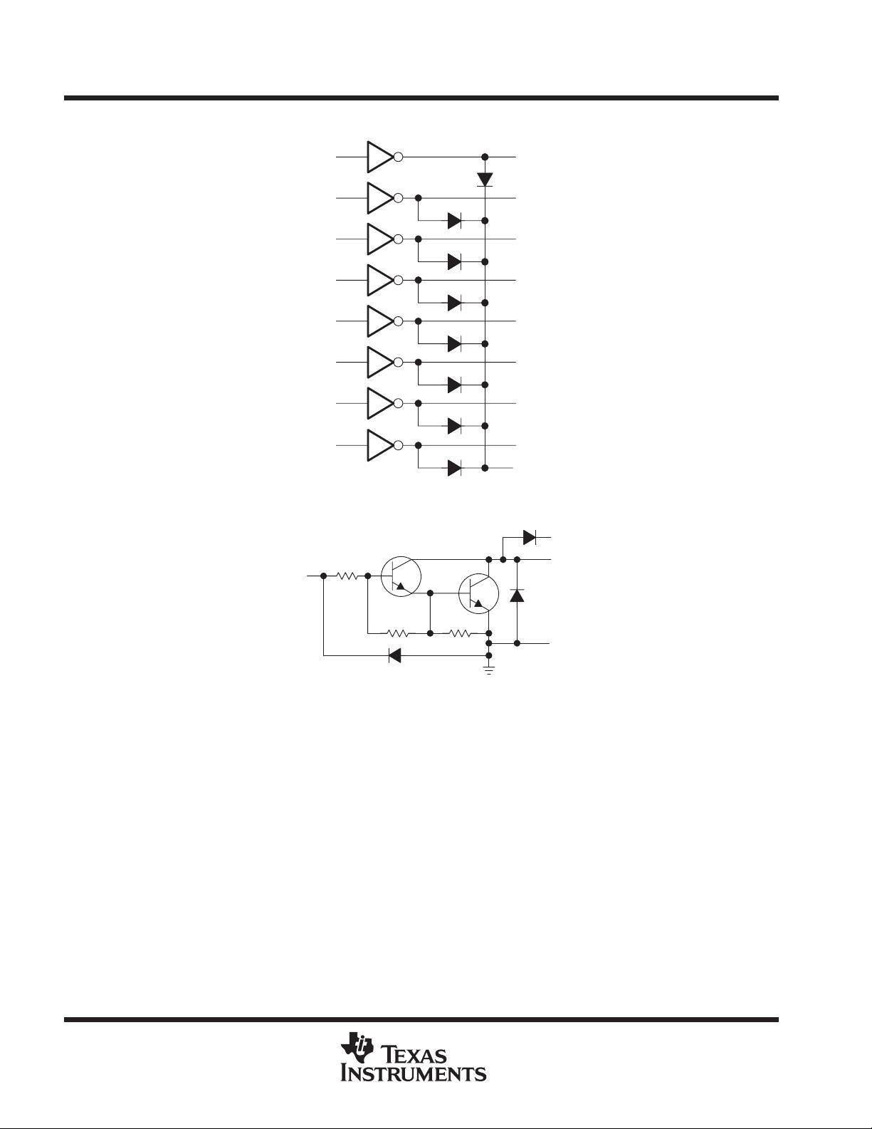
The ULN2803A is a high-voltage, high-current Darlington
transistor array. The device consists of eight npn Darlington pairs
that feature high-voltage outputs with common-cathode clamp
diodes for switching inductive loads. The collector-current rating of
each Darlington pair is 500 mA. The Darlington pairs may be
connected in parallel for higher current capability.
Applications include relay drivers, hammer drivers, lamp drivers, display drivers (LED and gas discharge), line
drivers, and logic buffers. The ULN2803A has a 2.7-kΩ series base resistor for each Darlington pair for operation
directly with TTL or 5-V CMOS devices.
ORDERING INFORMATION
T
A
PACKAGE
†
ORDERABLE
PART NUMBER
TOP-SIDE
MARKING
PDIP (N) Tube of 20 ULN2803AN ULN2803AN
−40°C to 85°C
SOIC (DW)
Tube of 40 ULN2803ADW
ULN2803A
−40 C to 85 C
SOIC (DW)
Reel of 2000 ULN2003ADWR
ULN2803A
†
Package drawings, standard packing quantities, thermal data, symbolization, and PCB design guidelines are
available at www.ti.com/sc/package.
Copyright 2004, Texas Instruments Incorporated
Please be aware that an important notice concerning availability, standard warranty, and use in critical applications of
Texas Instruments semiconductor products and disclaimers thereto appears at the end of this data sheet.
1
2
3
4
5
6
7
8
9
18
17
16
15
14
13
12
11
10
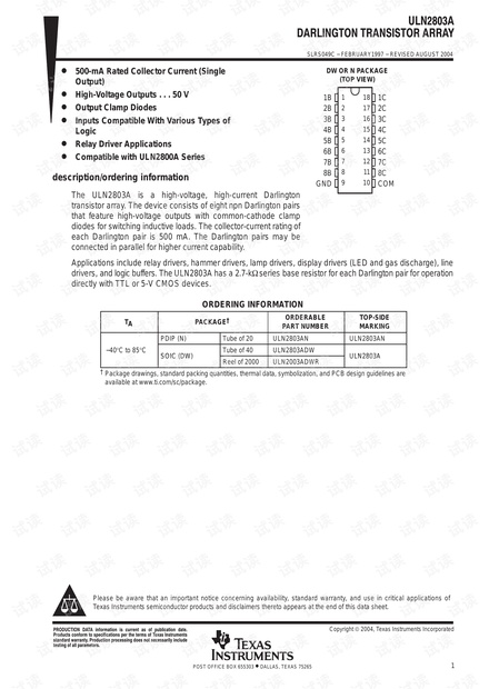
1B
2B
3B
4B
5B
6B
7B
8B
GND
1C
2C
3C
4C
5C
6C
7C
8C
COM
DW OR N PACKAGE
(TOP VIEW)
!" #$
# % &
## '($ # ) # "( "#
) "" $

剩余10页未读,继续阅读

ay172
- 粉丝: 0
- 资源: 3
 我的内容管理
收起
我的内容管理
收起
- 我的资源
快来上传第一个资源
 我的收益 登录查看自己的收益
 我的积分
登录查看自己的积分
我的积分
登录查看自己的积分
 我的C币
登录后查看C币余额
我的C币
登录后查看C币余额
 我的收藏
我的收藏  我的下载
我的下载  下载帮助
下载帮助

会员权益专享


最新资源
- RTL8188FU-Linux-v5.7.4.2-36687.20200602.tar(20765).gz
- c++校园超市商品信息管理系统课程设计说明书(含源代码) (2).pdf
- 建筑供配电系统相关课件.pptx
- 企业管理规章制度及管理模式.doc
- vb打开摄像头.doc
- 云计算-可信计算中认证协议改进方案.pdf
- [详细完整版]单片机编程4.ppt
- c语言常用算法.pdf
- c++经典程序代码大全.pdf
- 单片机数字时钟资料.doc
- 11项目管理前沿1.0.pptx
- 基于ssm的“魅力”繁峙宣传网站的设计与实现论文.doc
- 智慧交通综合解决方案.pptx
- 建筑防潮设计-PowerPointPresentati.pptx
- SPC统计过程控制程序.pptx
- SPC统计方法基础知识.pptx
资源上传下载、课程学习等过程中有任何疑问或建议,欢迎提出宝贵意见哦~我们会及时处理!
点击此处反馈


评论0