
ADV7180
Rev. F | Page 16 of 116
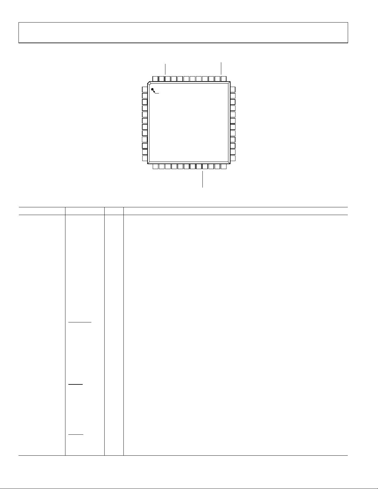
48-LEAD LQFP
48
NC
47
HS
46
INTRQ
45
VS/FIELD
44
DVDD
43
DGND
42
GPO2
41
GPO3
40
SCLK
39
SDATA
38
ALSB
37
RESET
35
A
IN
5
34
A
IN
4
33
A
IN
3
30
VFEFN
31
AVDD
32
AGND
36
A
IN
6
29
VREFP
28
AGND
27
A
IN
2
25
PVDD
26
A
IN
1
2
DVDDIO
3
SFL
4
DVDDIO
7
P7
6
GPO0
5
GPO1
1
DGND
8
P6
9
P5
10
P4
12
P2
11
P3
NC = NO CONNECT
13
DGND
14
LLC
15
NC
16
XTAL1
17
XTAL
18
DVDD
19
DGND
20
P1
21
PWRDWN
22
P0
23
AGND
24
ELPF
PIN 1
ADV7180
LQFP
TOP VIEW
(Not to Scale)
05700-062
Figure 11. 48-Lead LQFP Pin Configuration
Table 12. 48-Lead LQFP Pin Function Descriptions
Pin No. Mnemonic Type Description
1, 13, 19, 43 DGND G Digital Ground.
2, 4 DVDDIO P Digital I/O Supply Voltage (1.8V to 3.3 V).
3 SFL O
Subcarrier Frequency Lock. This pin contains a serial output stream that can be used to lock the
subcarrier frequency when this decoder is connected to any Analog Devices digital video encoder.
5, 6, 41, 42 GPO0 to GPO3 O General-Purpose Outputs. These pins can be configured via I
2
C to allow control of external devices.
7 to 12, 20, 22 P7 to P2, P1, P0 O Video Pixel Output Port. See Table 100 for output configuration for 8-bit and 16-bit modes.
14 LLC O
This is a line-locked output clock for the pixel data output by the ADV7180. It is nominally
27 MHz but varies up or down according to video line length.
15, 48 NC No Connect Pins. These pins are not connected internally.
16 XTAL1 O
This pin should be connected to the 28.6363 MHz crystal or left as a no connect if an external 1.8 V,
28.6363 MHz clock oscillator source is used to clock the ADV7180. In crystal mode, the crystal
must be a fundamental crystal.
17 XTAL I
This is the input pin for the 28.6363 MHz crystal, or this pin can be overdriven by an external 1.8 V,
28.6363 MHz clock oscillator source. In crystal mode, the crystal must be a fundamental crystal.
18, 44 DVDD P Digital Supply Voltage (1.8 V).
21
PWRDWN
I A logic low on this pin places the ADV7180 in power-down mode.
23, 28, 32 AGND G Analog Ground.
24 ELPF I The recommended external loop filter must be connected to the ELPF pin, as shown in Figure 58.
25 PVDD P PLL Supply Voltage (1.8 V).
26, 27, 33 to 36 A
IN
1 to A
IN
6 I Analog Video Input Channels.
29 VREFP O Internal Voltage Reference Output. See Figure 58 for recommended output circuitry.
30 VREFN O Internal Voltage Reference Output. See Figure 58 for recommended output circuitry.
31 AVDD P Analog Supply Voltage (1.8 V).
37
RESET
I
System Reset Input. Active low. A minimum low reset pulse width of 5 ms is required to reset
the ADV7180 circuitry.
38 ALSB I
This pin selects the I
2
C address for the ADV7180. For ALSB set to Logic 0, the address selected
for a write is 0x40; for ALSB set to Logic 1, the address selected is 0x42.
39 SDATA I/O I
2
C Port Serial Data Input/Output Pin.
40 SCLK I I
2
C Port Serial Clock Input. The maximum clock rate is 400 kHz.
45 VS/FIELD O Vertical Synchronization Output Signal/Field Synchronization Output Signal.
46
INTRQ
O
Interrupt Request Output. Interrupt occurs when certain signals are detected on the input video
(see Table 108).
47 HS O Horizontal Synchronization Output Signal.

剩余115页未读,继续阅读

weixin_38475690
- 粉丝: 0
- 资源: 5
 我的内容管理
收起
我的内容管理
收起
- 我的资源
快来上传第一个资源
 我的收益 登录查看自己的收益
 我的积分
登录查看自己的积分
我的积分
登录查看自己的积分
 我的C币
登录后查看C币余额
我的C币
登录后查看C币余额
 我的收藏
我的收藏  我的下载
我的下载  下载帮助
下载帮助

会员权益专享


最新资源
- VMP技术解析:Handle块优化与壳模板初始化
- C++ Primer 第四版更新:现代编程风格与标准库
- 计算机系统基础实验:缓冲区溢出攻击(Lab3)
- 中国结算网上业务平台:证券登记操作详解与常见问题
- FPGA驱动的五子棋博弈系统:加速与创新娱乐体验
- 多旋翼飞行器定点位置控制器设计实验
- 基于流量预测与潮汐效应的动态载频优化策略
- SQL练习:查询分析与高级操作
- 海底数据中心散热优化:从MATLAB到动态模拟
- 移动应用作业:MyDiaryBook - Google Material Design 日记APP
- Linux提权技术详解:从内核漏洞到Sudo配置错误
- 93分钟快速入门 LaTeX:从入门到实践
- 5G测试新挑战与罗德与施瓦茨解决方案
- EAS系统性能优化与故障诊断指南
- Java并发编程:JUC核心概念解析与应用
- 数据结构实验报告:基于不同存储结构的线性表和树实现
资源上传下载、课程学习等过程中有任何疑问或建议,欢迎提出宝贵意见哦~我们会及时处理!
点击此处反馈


