没有合适的资源?快使用搜索试试~ 我知道了~
首页TMS320C6713 GPIO指南:450MHz DSP的高级功能与应用
TMS320C6713 GPIO指南:450MHz DSP的高级功能与应用
需积分: 21 12 下载量 89 浏览量
更新于2023-06-04
1
收藏 212KB PDF 举报
本文档是关于TMS320C6713 Digital Signal Processor (DSP) 的GPIO指南,针对的是这款高性能的处理器,其主频高达450兆赫兹(MHz),具有出色的指令处理能力。C6713 DSP支持8级并行指令流水线设计,这意味着在任何时刻,它可以同时执行多达8条指令,这极大地提高了数据处理和系统性能。 GPIO,即通用目的输入/输出,是数字信号处理器中非常关键的功能,它允许处理器与外部设备进行直接交互,包括开关、传感器输入和驱动LED等。在TMS320C6713中,GPIO提供了丰富的接口资源,用户可以通过编程配置这些引脚作为输入或输出,实现灵活的数据传输和控制功能。 文档SPRU584A,发布于2004年3月,包含了详细的GPIO参考手册,涵盖了如何设置和管理这些输入/输出引脚的操作方式,如中断管理、线驱动能力、电源管理和信号配置等。值得注意的是,尽管该指南提供了重要的技术信息,但用户在使用前应确保获取最新的技术支持和规格,因为TI保留随时更新产品和服务的权利,并可能根据需求进行改动或停止某些产品。 此外,购买TI的产品和服务都受到其销售条款和条件的约束,硬件产品的保修仅限于销售时适用的规格,且并非所有参数都经过了全面测试。对于应用支持和客户产品设计,TI不承担法律责任,用户需自行负责确保产品的正确性和适应性。 TMS320C6713 DSP的GPIO指南为开发人员提供了一个强大而灵活的工具,用于构建高效能的嵌入式系统,但同时也强调了及时获取最新资料和充分理解责任划分的重要性。通过理解和利用这一指南,工程师能够充分利用C6713的GPIO功能,提升系统的可靠性和效率。
资源详情
资源推荐
![](https://csdnimg.cn/release/download_crawler_static/8680179/bg8.jpg)
8 General-Purpose Input/Output (GPIO) SPRU584A
This page is intentionally left blank.
![](https://csdnimg.cn/release/download_crawler_static/8680179/bg9.jpg)
9General-Purpose Input/Output (GPIO)SPRU584A
General-Purpose Input/Output (GPIO)
This document describes the general-purpose input/output (GPIO) peripheral
in the digital signal processors (DSPs) of the TMS320C6000 DSP family.
1 Overview
The general-purpose input/output (GPIO) peripheral provides dedicated
general-purpose pins that can be configured as either inputs or outputs. When
configured as an output, you can write to an internal register to control the state
driven on the output pin. When configured as an input, you can detect the state
of the input by reading the state of an internal register.
In addition, the GPIO peripheral can produce CPU interrupts and EDMA
events in different interrupt/event generation modes.
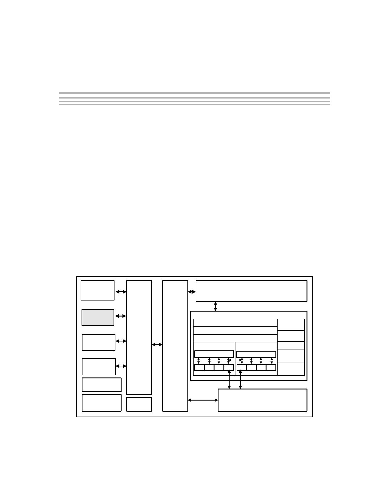
Figure 1 shows the GPIO peripheral in the TMS320C64x DSP. Figure 2
shows the GPIO peripheral block diagram.
Figure 1. TMS320C64x DSP Block Diagram
C6000 DSP core
Instruction Fetch
Instruction Dispatch
Instruction Decode
Data Path A
A Register File
L1 S1 M1 D1
Control
Registers
Control
Logic
Test
In−Circuit
Emulation
Interrupt
Control
Data Path B
B Register File
L2S2M2D2
L1P Cache
L2
Memory
L1D Cache
Enhanced
DMA
Controller
Power Down
Logic
EMIF
Other
Peripherals
Boot
Configuration
Interrupt
Selector
PLL
GPIO
剩余41页未读,继续阅读
![pdf](https://img-home.csdnimg.cn/images/20210720083512.png)
![text/plain](https://img-home.csdnimg.cn/images/20210720083646.png)
![](https://csdnimg.cn/download_wenku/file_type_ask_c1.png)
安全验证
文档复制为VIP权益,开通VIP直接复制
![](https://csdnimg.cn/release/wenkucmsfe/public/img/green-success.6a4acb44.png)