

ADC
RF_P,N
Program
Flash
128/192 kB
Data
RAM
12 kB
HF crystal
OSC
LF crystal
OSC
General
Purpose
ADC
Serial
Wire and
JTAG
debug
Internal LF
RC-OSC
GPIO multiplexor switch
Chip
manager
1.8V
Regulator
Bias
2
nd
level
Interrupt
controller
RF_TX_ALT_P,N
OSCA
OSCB
PA[7:0], PB[7:0], PC[7:0]
Encryption
acclerator
IF
Always
Powered
Domain
ARM
®
Cortex
TM
-M3
CPU with NVIC
and MPU
VREG_OUT
Watchdog
PA select
LNA
PA
PA
DAC
MAC
+
Baseband
Sleep
timer
POR
nRESET
General
purpose
timers
GPIO
registers
UART/
SPI/TWI
SYNTH
Internal HF
RC-OSC
TX_ACTIVE
SWCLK,
JTCK
Calibration
ADC
Packet Trace
CPU debug
TPIU/ITM/
FPB/DWT
1.25V
Regulator
VDD_CORE
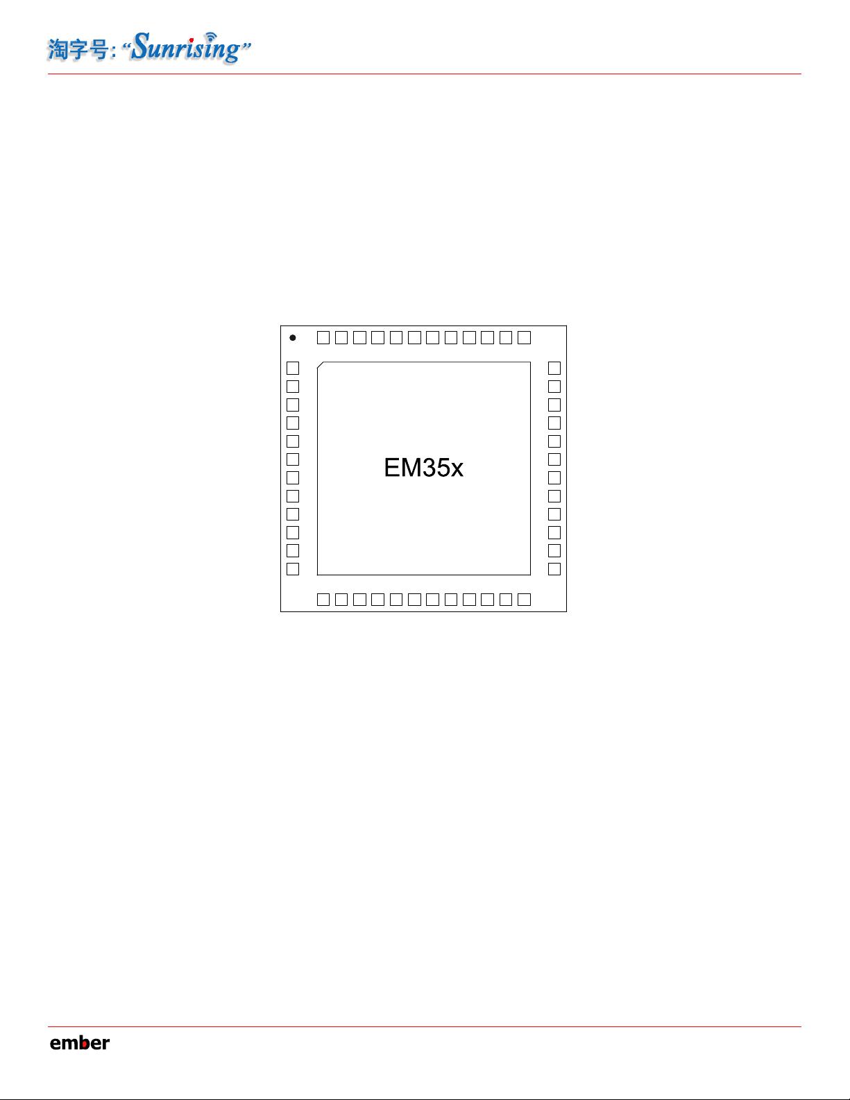
EM351 / EM357
High-Performance, Integrated ZigBee/802.15.4 System-on-Chip
Complete System-on-Chip
•
32-bit ARM
®
Cortex™-M3 processor
•
2.4 GHz IEEE 802.15.4-2003 transceiver & lower
MAC
•
128 or 192 kB flash, with optional read
protection
•
12 kB RAM memory
•
AES128 encryption accelerator
•
Flexible ADC, UART/SPI/TWI serial
communications, and general purpose timers
•
24 highly configurable GPIOs with Schmitt
trigger inputs
Industry-leading ARM
®
Cortex
™
-M3 processor
•
Leading 32-bit processing performance
•
Highly efficient Thumb-2 instruction set
•
Operation at 6, 12, or 24 MHz
•
Flexible Nested Vectored Interrupt Controller
Low power consumption, advanced management
•
Rx Current (w/ CPU): 26 mA
•
Tx Current (w/ CPU, +3 dBm TX): 31 mA
•
Low deep sleep current, with retained RAM and
GPIO: 400 nA without/800 nA with sleep timer
•
Low-frequency internal RC oscillator for low-
power sleep timing
•
High-frequency internal RC oscillator for fast
(110 µsec) processor start-up from sleep
Exceptional RF Performance
•
Normal mode link budget up to 103 dB;
configurable up to 110 dB
•
-100 dBm normal RX sensitivity;
configurable to -102 dBm
(1% PER, 20 byte packet)
•
+3 dB normal mode output power;
configurable up to +8 dBm
•
Robust Wi-Fi and Bluetooth coexistence
Innovative network and processor debug
•
Ember InSight port for non-intrusive
packet trace with Ember InSight tools
•
Serial Wire/JTAG interface
•
Standard ARM debug capabilities: Flash
Patch & Breakpoint; Data Watchpoint &
Trace; Instrumentation Trace Macrocell
Application Flexibility
•
Single voltage operation: 2.1-3.6 V
with internal 1.8 V and 1.25 V regulators
•
Optional 32.768 kHz crystal for higher
timer accuracy
•
Low external component count with
single 24 MHz crystal
•
Support for external power amplifier
•
Small 7x7 mm 48-pin QFN package
Ember Corporation
47 Farnsworth Street
Boston MA 02210 USA
+1 617.951.0200
www.ember.com
120-035X-000D
Preliminary
November 20, 2009


剩余239页未读,继续阅读

qq_20026077
- 粉丝: 0
- 资源: 2
 我的内容管理
收起
我的内容管理
收起
- 我的资源
快来上传第一个资源
 我的收益 登录查看自己的收益
 我的积分
登录查看自己的积分
我的积分
登录查看自己的积分
 我的C币
登录后查看C币余额
我的C币
登录后查看C币余额
 我的收藏
我的收藏  我的下载
我的下载  下载帮助
下载帮助

会员权益专享


最新资源
- BSC绩效考核指标汇总 (2).docx
- BSC资料.pdf
- BSC绩效考核指标汇总 (3).pdf
- C5000W常见问题解决方案.docx
- BSC概念 (2).pdf
- ESP8266智能家居.docx
- ESP8266智能家居.pdf
- BSC概念 HR猫猫.docx
- C5000W常见问题解决方案.pdf
- BSC模板:关键绩效指标示例(财务、客户、内部运营、学习成长四个方面).docx
- BSC概念.docx
- BSC模板:关键绩效指标示例(财务、客户、内部运营、学习成长四个方面).pdf
- BSC概念.pdf
- 各种智能算法的总结汇总.docx
- BSC概念 HR猫猫.pdf
- bsc概念hr猫猫.pdf
资源上传下载、课程学习等过程中有任何疑问或建议,欢迎提出宝贵意见哦~我们会及时处理!
点击此处反馈


