没有合适的资源?快使用搜索试试~ 我知道了~
首页STK682-010-E秒杀替换THB7128 直接替换
STK682-010-E秒杀替换THB7128 直接替换
需积分: 50 13 下载量 62 浏览量
更新于2023-06-10
评论
收藏 1.07MB PDF 举报
高细分、大功率两相混合式步进电机驱动芯片 特性 ● 双全桥MOSFET驱动,低导通电阻Ron=0.53Ω ● 最高耐压40VDC,大电流3.3 A(峰值) ● 多种细分可选(1、1/2、1/4、1/8、1/16、1/32、1/64、1/128) ● 自动半流锁定功能 ● 内置混合式衰减模式 ● 内置输入下拉电阻 ● 内置温度保护及过流保护
资源详情
资源评论
资源推荐
RoHS DIRECTIVE PASS 018-13-00**
130228HI No.1
Preliminary Datasheet
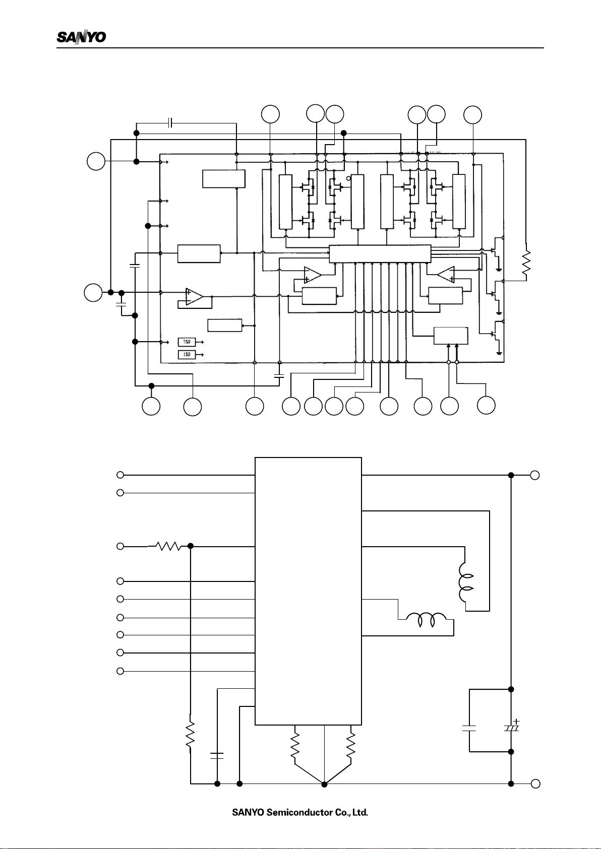
Product Name STK682-010-E
1.Case Outline:19 pins (See attached case outline dimensions.)
2.Function :PWM current control stepping motor driver
3.Application :Industrial equipment etc.
4.Features:
・Output on-resistance (High side 0.3 Ω, Low side 0.25 Ω, Total 0.55 Ω; Ta = 25℃, I
O
= 2.5A)
・VMmax=36V(DC),Iopmax=3.0A
・2, 1-2, W1-2, 2W1-2, 4W1-2, 8W1-2, 16W1-2, 32W1-2 phase excitation are selectable
・With built-in automatic half current maintenance energizing function
・Over current protection circuit
・Thermal shutdown circuit
・Input pull down resistance
・With reset pin and enable pin
5.Absolute Maximum Ratings/Tc=25℃
Parameter
Symbol
Conditions
Ratings
Unit
supply voltage
VMmax
36
V
Peak output current
Iopmax
3.0
A
Logic input voltage
VINmax
6
V
VREF input voltage
VREFmax
6
V
Operating substrate temperature
Tc
-20 to +105
℃
Storage temperature
Tstg
-40 to +125
℃
6.Allowable Operating Ranges/Ta=25℃
Parameter
Symbol
Conditions
Ratings
Unit
Supply voltage range
VM
9 to 32
V
Logic input voltage range
VIN
0 to 5
V
VCC input voltage range
VCC
0 to 5
V
VREF input voltage range
VREF
0 to 3
V
Output current1
Io1
1-2Phase-ex,Tc≦90℃
3.0
A
Output current2
Io2
1-2Phase-ex,Tc=105℃
2.5
A
Output current3
Io3
2Phase-ex,Tc=105℃
1.8
A
STK682-010-E
018-13-00**
130228HI No.2
7.Electrical Characteristics/Tc=25℃, VM=24V
Parameter
Symbol
Conditions
Ratings
Unit
min.
typ.
max.
Standby mode current drain
IMstn
VCC=”L”
70
100
μA
Current drain
IM
VCC=”H”,ENABLE="H"
No Load
3.3
4.6
mA
Thermal shutdown temperature
TSD
Design guarantee
150
180
210
℃
Thermal hysteresis width
ΔTSD
Design guarantee
40
℃
Logic pin input current
IinL1
VIN=0.8V
3
8
15
μA
IinH1
VIN=5V
30
50
70
μA
Logic input high-level voltage
Vinh
Pins 2,3,16,17,18,19
2.0
V
Logic input low-level voltage
Vinl
Pins 2,3,16,17,18,19
0.8
V
FDT pin high-level voltage
Vfdth
Pin 6
3.5
V
FDT pin middle-level voltage
Vfdtm
Pin 6
1.1
3.1
V
FDT pin low-level voltage
Vfdtl
Pin 6
0.8
V
Chopping frequency
Fch
C1=100pF
58
83
108
kHz
Chopping frequency
Iosc1
10
μA
Chopping oscillator circuit
threshold voltage
Vtup1
1
V
Vtdown1
0.5
V
VREF pin input voltage
Iref
VREF=1.5V,CLK=10kHz
-0.5
μA
DOWN output residual voltage
VolDO
Idown=1mA,CLK=Low
40
mV
Hold current switching frequency
Falert
1.6
Hz
Blanking time
Tb1
1
μs
Output block
Output on-resistance
Ronu
I
O
=2.0A, high-side ON resistance
0.30
0.42
Ω
Rond
I
O
=2.0A, low-side ON resistance
0.25
0.35
Ω
Output leakage current
Ioleak
VM=36V
50
μA
Diode forward voltage
VD
ID=-2.0A
1.1
1.4
V
Current setting reference voltage
VRF
VREF=1.5V, Current ratio 100%
300
mV
Output short-circuit protection block
Timer latch time
Tscp
256
μs
STK682-010-E
018-13-00**
130228HI No.3
8. Block diagram
9.Application Circuit Example
2
3
15
5
16
18
17
19
8
4
6
12
14
7
9
11
13
M3
M2
M1
VCC
CLK
5V
VREF
OSC1
FDT
NFB
NFA
VM
OUT2B
OUT1B
OUT2A
OUT1A
C1
RFB
RFA
R2
R1
C2
C3
STK682-010-E
GND
VM=24V
1
GND
10
PGND
CW/CCW
ENABLE
M3
M1
VM
NFB
DOWN
VCC
ENABLE
M2
OUT1A
OUT1B
19
17
15
11
8
VREF
5
OSC1
CW/CCW
2
18
16
14
12
9
7
CLK
3
13
GND
1
PGND
10
NFA
VREG2
PGND
A
PGND
B
VREG1
OSC2
Output pre stage
Output pre stage
Regulator 2
Regulator 1
Current select
circuit
Output pre stage
Output pre stage
Output control logic
Current select
circuit
Decay Mode
setting circuit
Oscillator
OUT2A
OUT2B
4
6
FDT
1.2k
STK682-010-E
018-13-00**
130228HI No.4
10.Pin Functions
Pin No.
Pin symbol
Pin Functions
1
GND
Circuit GND
2
CW/CCW
Forward / Reverse signal input
3
CLK
Clock pulse signal input
4
OSC1
Chopping frequency setting capacitor connection
5
VREF
Constant-current control reference voltage input
6
FDT
Decay mode select voltage input
7
OUT2B
B phase OUTB output
8
NFB
B phase current sense resistance connection
9
OUT1B
B phase OUTA output
10
PGND
Power GND
11
OUT2A
A phase OUTB output
12
NFA
A phase current sense resistance connection
13
OUT1A
A phase OUTA output
14
VM
Motor supply connection
15
VCC
Chip enable input
16
M1
Excitation-mode switching pin
17
M2
18
M3
19
ENABLE
Output enable signal input
剩余18页未读,继续阅读
丘风1
- 粉丝: 0
- 资源: 2
上传资源 快速赚钱
- 我的内容管理 收起
- 我的资源 快来上传第一个资源
- 我的收益 登录查看自己的收益
- 我的积分 登录查看自己的积分
- 我的C币 登录后查看C币余额
- 我的收藏
- 我的下载
- 下载帮助
会员权益专享
最新资源
- RTL8188FU-Linux-v5.7.4.2-36687.20200602.tar(20765).gz
- c++校园超市商品信息管理系统课程设计说明书(含源代码) (2).pdf
- 建筑供配电系统相关课件.pptx
- 企业管理规章制度及管理模式.doc
- vb打开摄像头.doc
- 云计算-可信计算中认证协议改进方案.pdf
- [详细完整版]单片机编程4.ppt
- c语言常用算法.pdf
- c++经典程序代码大全.pdf
- 单片机数字时钟资料.doc
- 11项目管理前沿1.0.pptx
- 基于ssm的“魅力”繁峙宣传网站的设计与实现论文.doc
- 智慧交通综合解决方案.pptx
- 建筑防潮设计-PowerPointPresentati.pptx
- SPC统计过程控制程序.pptx
- SPC统计方法基础知识.pptx
资源上传下载、课程学习等过程中有任何疑问或建议,欢迎提出宝贵意见哦~我们会及时处理!
点击此处反馈
安全验证
文档复制为VIP权益,开通VIP直接复制
信息提交成功
评论0