
1996 Microchip Technology Inc.
Preliminary
DS21170A-page 1
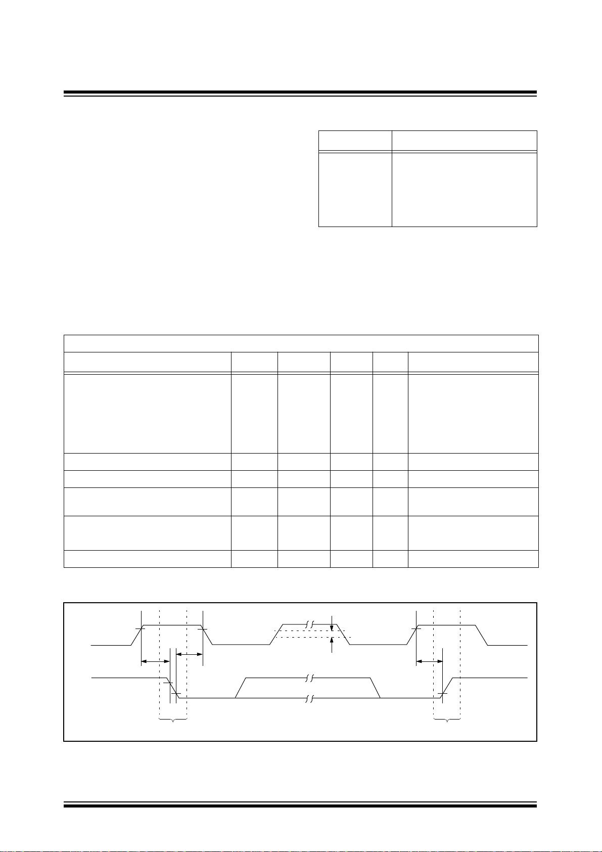
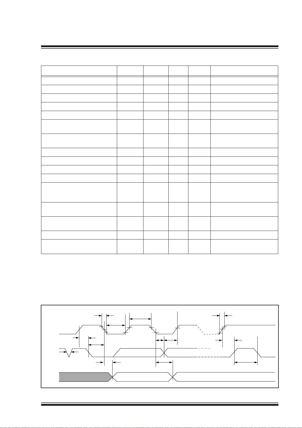
FEATURES
• ISO Standard 7816 pad locations
• Low power CMOS technology
- 1 mA active current typical
- 10
µ
A standby current typical at 5.5V
• Organized as a single block of 128 bytes (128 x 8)
or 256 bytes (256 x 8)
• Two-wire serial interface bus, I
2
C
compatible
• 100 kHz and 400 kHz compatibility
• Self-timed write cycle (including auto-erase)
• Page-write buffer for up to 8 bytes
• 2 ms typical write cycle time for page-write
• ESD protection > 4 kV
• 1,000,000 E/W cycles guaranteed
• Data retention > 200 years
• Available for extended temperature ranges
DESCRIPTION
The Microchip Technology Inc. 24C01SC and
24C02SC are 1K-bit and 2K-bit Electrically Erasable
PROMs with bondpad positions optimized for smart
card applications. The devices are organized as a sin-
gle block of 128 x 8-bit or 256 x 8-bit memory with a
two-wire serial interface. The 24C01SC and 24C02SC
also have page-write capability for up to 8 bytes of data.
- Commercial (C): 0
°
C to +70
°
C
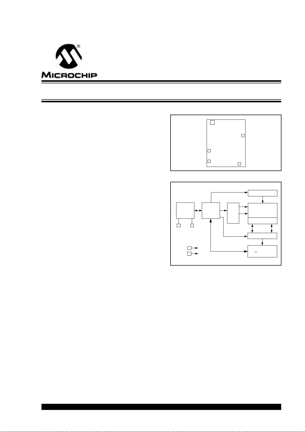
DIE LAYOUT
BLOCK DIAGRAM
SDA
DC
V
CC
SCL
V
SS
HV GENERATOR
EEPROM
ARRAY
PAGE LATCHES
YDEC
XDEC
SENSE AMP
R/W CONTROL
MEMORY
CONTROL
LOGIC
I/O
CONTROL
LOGIC
SDA SCL
VCC
VSS
1K/2K 5.0V I
2
C Serial EEPROMs for Smart Cards
24C01SC/02SC
I
2
C is a trademark of Philips Corporation.
This document was created with FrameMaker404
剩余12页未读,继续阅读


