没有合适的资源?快使用搜索试试~ 我知道了~
首页Constraining and Analyzing Source-Synchronous Interfaces
Constraining and Analyzing Source-Synchronous Interfaces
需积分: 15 11 下载量 53 浏览量
更新于2023-07-05
评论 1
收藏 1.92MB PDF 举报
这是altera公司对SDR/DDR源同步接口进行时序约束的资料,很有用。
资源详情
资源评论
资源推荐
© March 2010 Altera Corporation AN 433: Constraining and Analyzing Source-Synchronous Interfaces
AN-433-2.2© March 2010
AN 433: Constraining and Analyzing
Source-Synchronous Interfaces
This application note describes techniques for constraining and analyzing
source-synchronous interfaces. In source-synchronous interfaces, the source of the
clock is the same device as the source of the data, rather than another source, such as a
common clock network.
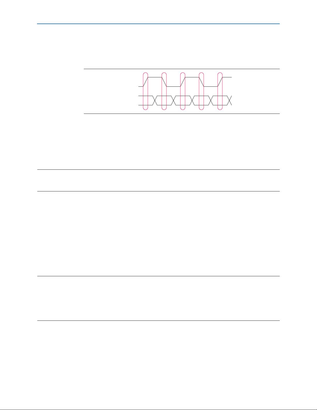
Figure 1 shows a block diagram of a basic source-synchronous interface.
Introduction
Source-synchronous interfaces are used for high-speed data transfer. DDR memory,
HyperTransport buses, and the SPI-4.2 standard all use source-synchronous
interfaces.
Constraining source-synchronous interfaces can be complex. The Synopsys Design
Constraints (SDC) format provides the necessary detail and precision for a proper
analysis. Familiarize yourself with the SDC format and the TimeQuest timing
analyzer before you read this application note.
f For more information, refer to the SDC and TimeQuest API Reference Manual and the
Quartus II TimeQuest Timing Analyzer chapter of the Quartus II Handbook.
This application note is divided into two main sections:
■ “Source-Synchronous Outputs” on page 6
■ “Source-Synchronous Inputs” on page 42
These sections include descriptions of the output and input interfaces and details
about the three types of SDC constraints or exceptions that apply to each direction.
You can use a script included with the Quartus
®
II software installation to guide you
through the process of creating constraints for source-synchronous interfaces. To use
the script, type the following command in your project directory:
quartus_sta --ssc <project name>
Figure 1. Basic Source-Synchronous Interface
Transmitter Receiver
Data
Clock Signal
Clock
Page 2 Introduction
AN 433: Constraining and Analyzing Source-Synchronous Interfaces © March 2010 Altera Corporation
Clock and Data Relationship
Some source-synchronous interfaces use a clock that is edge-aligned with the data, as
shown in Figure 2. When a clock is edge-aligned with the data, the receiving device
shifts the clock as necessary to capture the data. Some interfaces capture data after the
first rising or falling clock edge. Therefore, further logic is required in addition to a
clock shift after the first rising or falling latch edge.
Other source-synchronous interfaces use a clock that is shifted with respect to the data
(typically center-aligned with the data), as shown in Figure 3. The receiving device
directly uses the shifted clock to capture the data, especially in low-speed interfaces.
When a source-synchronous input clock directly latches the data, the receiving device
does not perform any extra clock alignment. However, in some interfaces, a
phase-locked loop (PLL) shifts the input clock, which is then used to latch the data. If
a PLL shifts the input clock, you can adjust the clock and data timing relationship by
adjusting the PLL phase offset.
SDR (Single Data Rate) and DDR (Double Data Rate)
In source-synchronous SDR interfaces, one edge of the clock, typically the rising edge,
transfers the data, as shown in Figure 4. The time required to transmit one bit, known
as the unit interval (UI), is equal to the period of the clock.
Figure 2. Edge-Aligned Clock and Data
Figure 3. Center-Aligned Clock and Data
data
clock
data
clock
Figure 4. SDR Capture
clock
data
Introduction Page 3
© March 2010 Altera Corporation AN 433: Constraining and Analyzing Source-Synchronous Interfaces
In source-synchronous DDR interfaces, data is transferred on both edges of the clock,
as shown in Figure 5. The UI is equal to half the period of the clock, assuming a 50/50
duty cycle.
Data constraints are necessary for each active clock edge. SDR interfaces require
constraints for only one active clock edge, typically the rising edge. DDR interfaces
require constraints that are relative to the rising and falling clock edges.
Example 1 shows constraints that are relative to the rising clock edge. For an SDR
interface, no other data constraints are necessary.
A DDR interface requires data constraints that are relative to the falling and rising
edges of the clock.
When you make data constraints for DDR interfaces, duplicate the constraints that are
relative to the rising clock edge, and add the -clock_fall and -add_delay
options so the constraints are relative to the falling clock edge.
Example 2 shows data constraints that are relative to the rising and falling clock
edges. The -clock_fall option makes the constraint relative to the falling clock
edge, and the -add_delay option allows multiple maximum or minimum delay
constraints to apply to the same port.
Figure 5. DDR Capture
clock
data
Example 1. Sample Output Constraints for an SDR Interface
set_output_delay -clock [get_clocks output_clk] -max 2 [get_ports data_out]
set_output_delay -clock [get_clocks output_clk] -min -1 \
[get_ports data_out] -add_delay
Example 2. Sample Output Constraints for a DDR Interface
set_output_delay -clock [get_clocks output_clk] -max 2 [get_ports data_out]
set_output_delay -clock [get_clocks output_clk] -min -1 \
[get_ports data_out] -add_delay
set_output_delay -clock [get_clocks output_clk] -max 2 -clock_fall \
[get_ports data_out] -add_delay
set_output_delay -clock [get_clocks output_clk] -min -1 -clock_fall \
[get_ports clk_in] -add_delay
Page 4 Introduction
AN 433: Constraining and Analyzing Source-Synchronous Interfaces © March 2010 Altera Corporation
Interface Constraints
Source-synchronous interfaces require the following three types of SDC constraints or
exceptions:
■ Clock constraints—Define the clocks used in the interface. Clock constraints
define the period and include any other clock characteristics such as offset and
uncertainty.
■ Input or output delay constraints—Describe the required times for data to be
valid at the interface. Input and output delay constraints are derived from timing
parameters, such as skew, t
SU
, or t
CO
that specify the interface operation.
There are two methods for deriving input and output delays for
source-synchronous interfaces based on the available or specified I/O timing:
■ System-centric method—Takes into account the timing information for the
FPGA as part of a larger system. Such timing information includes board trace
delays and I/O timing requirements of the external device to which the FPGA
interfaces. You can create constraints to describe these delays that are part of
the system outside the FPGA. Use the system-centric method when you have
timing information about the system with which the FPGA interfaces, or if you
want to verify the system timing on that interface.
■ FPGA-centric (or data sheet) method—Focuses on the clock and data
relationship at the boundary of the FPGA. This method does not require any
information about timing parameters outside the FPGA, such as board trace
delays and I/O timing requirements of external devices. You can create
constraints to specify the maximum acceptable skew across the data bus, and
the timing relationship between the data and clock signals (center or edge
alignment, for example). Use the FPGA-centric method when you constrain the
source-synchronous interface for a specific skew and clock and data
relationship. You can also use the FPGA-centric approach when you do not
know the external device timing parameters.
■ Timing exceptions—Control launch and latch edges used in timing analysis.
Timing exceptions ensure that valid timing paths in the interface are analyzed, and
invalid paths are not analyzed. For more information about why timing exceptions
are necessary, refer to “Default Timing Analysis Behavior”.
Default Timing Analysis Behavior
By default, timing analysis operates on the assumption that data launched by the
rising clock edge is latched by the next rising clock edge. Source-synchronous
interfaces, however, often exhibit different behavior. Data may be latched by the same
edge that launches it, and source-synchronous DDR interfaces launch and latch data
on rising and falling clock edges.
Introduction Page 5
© March 2010 Altera Corporation AN 433: Constraining and Analyzing Source-Synchronous Interfaces
Figure 6 shows the setup relationships analyzed by default in an edge-aligned DDR
interface. Solid red arrows indicate same-edge transfers (rise-to-rise and fall-to-fall),
and dashed red arrows indicate opposite-edge transfers (rise-to-fall and fall-to-rise).
Figure 7 shows the hold relationships analyzed by default in an edge-aligned DDR
interface. Solid blue arrows indicate hold relationships for same-edge transfers
(rise-to-rise and fall-to-fall), and dashed blue arrows indicate hold relationships for
opposite-edge transfers (rise-to-fall and fall-to-rise).
Figure 8 shows the setup relationships analyzed by default in a center-aligned DDR
interface. Solid red arrows indicate same-edge transfers (rise-to-rise and fall-to-fall),
and dashed red arrows indicate opposite-edge transfers (rise-to-fall and fall-to-rise).
Figure 6. Setup Relationships in an Edge-Aligned DDR Interface
Figure 7. Hold Relationships in an Edge-Aligned DDR Interface
Figure 8. Setup Relationships in a Center-Aligned DDR Interface
Launch Clock
Latch Clock
Launch Clock
Latch Clock
Launch Clock
Latch Clock
剩余58页未读,继续阅读
hyh_huang
- 粉丝: 0
- 资源: 2
上传资源 快速赚钱
- 我的内容管理 收起
- 我的资源 快来上传第一个资源
- 我的收益 登录查看自己的收益
- 我的积分 登录查看自己的积分
- 我的C币 登录后查看C币余额
- 我的收藏
- 我的下载
- 下载帮助
会员权益专享
最新资源
- zigbee-cluster-library-specification
- JSBSim Reference Manual
- c++校园超市商品信息管理系统课程设计说明书(含源代码) (2).pdf
- 建筑供配电系统相关课件.pptx
- 企业管理规章制度及管理模式.doc
- vb打开摄像头.doc
- 云计算-可信计算中认证协议改进方案.pdf
- [详细完整版]单片机编程4.ppt
- c语言常用算法.pdf
- c++经典程序代码大全.pdf
- 单片机数字时钟资料.doc
- 11项目管理前沿1.0.pptx
- 基于ssm的“魅力”繁峙宣传网站的设计与实现论文.doc
- 智慧交通综合解决方案.pptx
- 建筑防潮设计-PowerPointPresentati.pptx
- SPC统计过程控制程序.pptx
资源上传下载、课程学习等过程中有任何疑问或建议,欢迎提出宝贵意见哦~我们会及时处理!
点击此处反馈
安全验证
文档复制为VIP权益,开通VIP直接复制
信息提交成功
评论0