
MAX17040/MAX17041
Compact, Low-Cost 1S/2S Fuel Gauges
_______________________________________________________________________________________ 3
Note 1: All voltages are referenced to GND.
Note 2: SDA, SCL = GND; EO, SEO idle.
Note 3: External time base on EO pin must meet this specification.
Note 4: The MAX17040/MAX17041 enter Sleep mode 1.75s to 2.5s after (SCL < V
IL
) AND (SDA < V
IL
).
Note 5: f
SCL
must meet the minimum clock low time plus the rise/fall times.
Note 6: The maximum t
HD:DAT
has only to be met if the device does not stretch the low period (t
LOW
) of the SCL signal.
Note 7: This device internally provides a hold time of at least 75ns for the SDA signal (referred to the V
IHMIN
of the SCL signal) to
bridge the undefined region of the falling edge of SCL.
Note 8: Filters on SDA and SCL suppress noise spikes at the input buffers and delay the sampling instant.
Note 9: C
B
—total capacitance of one bus line in pF.
Note 10: Applies to 8-pin TDFN-EP package type only.
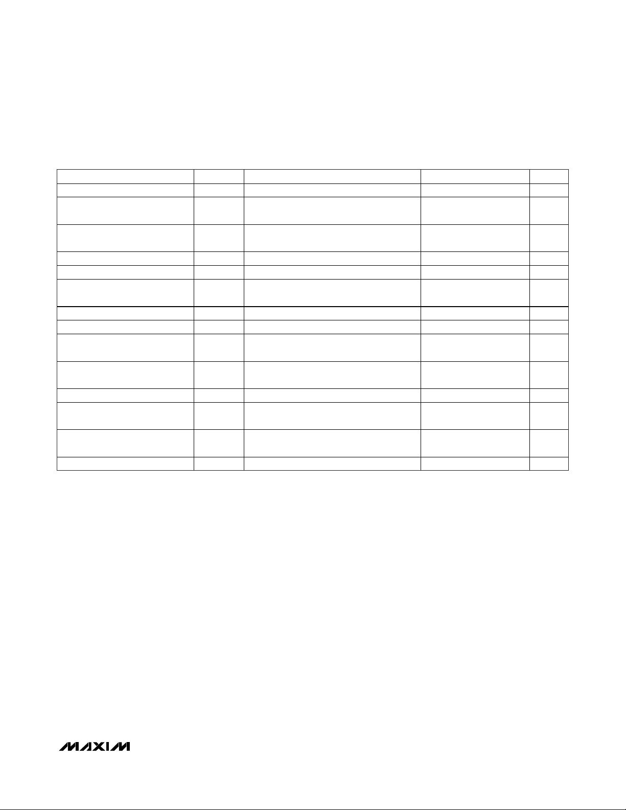
PARAMETER SYMBOL CONDITIONS MIN TYP MAX UNITS
SCL Clock Frequency f
SCL
(Note 5) 0 400 kHz
Bus Free Time Between a STOP
and START Condition
t
BUF
1.3 µs
Hold Time (Repeated)
START Condition
t
HD:STA
(Note 5) 0.6 µs
Low Period of SCL Clock t
LOW
1.3 µs
High Period of SCL Clock t
HIGH
0.6 µs
Setup Time for a Repeated
START Condition
t
SU:STA
0.6 µs
Data Hold Time t
HD:DAT
(Notes 6, 7) 0 0.9 µs
Data Setup Time t
SU:DAT
(Note 6) 100 ns
Rise Time of Both SDA
and SCL Signals
t
R
20 +
0.1C
B
300 ns
Fall Time of Both SDA
and SCL Signals
t
F
20 +
0.1C
B
300 ns
Setup Time for STOP Condition t
SU:STO
0.6 µs
Spike Pulse Widths Suppressed
by Input Filter
t
SP
(Note 8) 0 50 ns
Capacitive Load for Each
Bus Line
C
B
(Note 9) 400 pF
SCL, SDA Input Capacitance C
BIN
60 pF
ELECTRICAL CHARACTERISTICS: 2-WIRE INTERFACE
(2.5V ≤ V
DD
≤ 4.5V, T
A
= -20°C to +70°C.)
剩余12页未读,继续阅读

china_tongxin
- 粉丝: 4
- 资源: 5
 我的内容管理
收起
我的内容管理
收起
- 我的资源
快来上传第一个资源
 我的收益 登录查看自己的收益
 我的积分
登录查看自己的积分
我的积分
登录查看自己的积分
 我的C币
登录后查看C币余额
我的C币
登录后查看C币余额
 我的收藏
我的收藏  我的下载
我的下载  下载帮助
下载帮助

会员权益专享


最新资源
- 谷歌文件系统下的实用网络编码技术在分布式存储中的应用
- 跨国媒体对南亚农村社会的影响:以斯里兰卡案例的社会学分析
- RFM2g接口驱动操作手册:API与命令行指南
- 基于裸手的大数据自然人机交互关键算法研究
- ABAQUS下无人机机翼有限元分析与局部设计研究
- TCL基础教程:语法、变量与操作详解
- FPGA与数字前端面试题集锦:流程、设计与Verilog应用
- 2022全球互联网技术人才前瞻:元宇宙驱动下的创新与挑战
- 碳排放权交易实战手册(第二版):设计与实施指南
- 2022新经济新职业洞察:科技驱动下的百景变革
- 红外与可见光人脸融合识别技术探究
- NXP88W8977:2.4/5 GHz 双频 Wi-Fi4 + Bluetooth 5.2 合体芯片
- NXP88W8987:集成2.4/5GHz Wi-Fi 5与蓝牙5.2的单芯片解决方案
- TPA3116D2DADR: 单声道数字放大器驱动高达50W功率
- TPA3255-Q1:315W车载A/D类音频放大器,高保真、宽频设计
- 42V 输入 5A 降压稳压器 TPS54540B-Q1 的特点和应用
资源上传下载、课程学习等过程中有任何疑问或建议,欢迎提出宝贵意见哦~我们会及时处理!
点击此处反馈


