没有合适的资源?快使用搜索试试~ 我知道了~
首页TB6560中午PDF资料
TB6560中午PDF资料
4星 · 超过85%的资源 需积分: 9 80 下载量 96 浏览量
更新于2023-07-08
评论 1
收藏 426KB PDF 举报
难找的东东,如果想深入了解怎么驱动电机的,还是必须的,如果不想看英文的PDF资料的话,这是首选
资源详情
资源评论
资源推荐
TB6560HQ/FG
2006-05-31
1
TOSHIBA BiCD Integrated Circuit Silicon Monolithic
TB6560HQ,TB6560FG
PWM Chopper-Type bipolar
Stepping Motor Driver IC
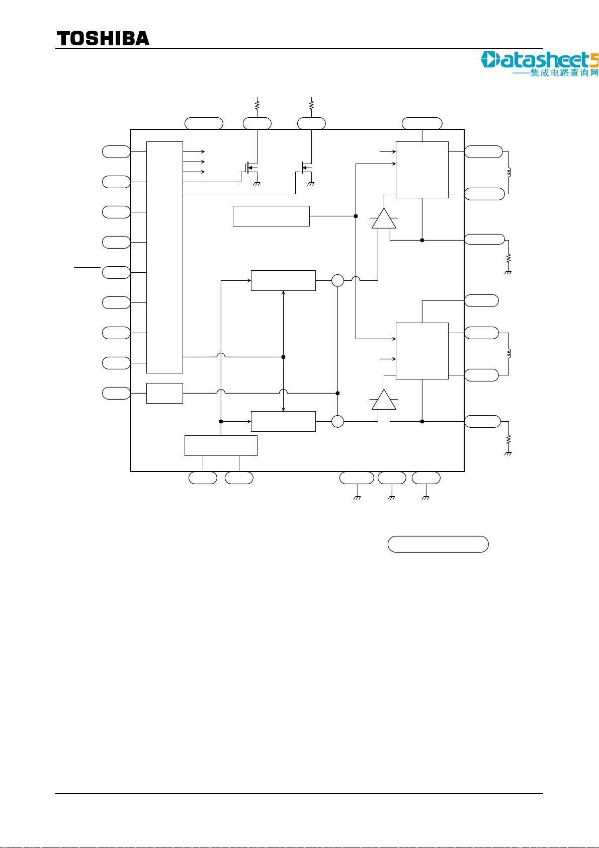
The TB6560HQ/FG is a PWM chopper-type sinusoidal micro-step
bipolar stepping motor driver IC.
It supports both 2-phase/1-2-phase/W1-2-phase/2W1-2-phase
excitation mode and forward/reverse mode and is capable of
low-vibration, high-performance drive of 2-phase bipolar type
stepping motors using only a clock signal.
Features
• Single-chip bipolar sinusoidal micro-step stepping motor
driver
• Uses high withstand voltage BiCD process:
Ron (upper lower) = 0.6 Ω (typ.)
• Forward and reverse rotation control available
• Selectable phase drive (2, 1-2, W1-2, and 2W1-2)
• High output withstand voltage: V
CEO
= 40 V
• High output current: I
OUT
= HQ: 3.5 A (peak)
FG: 2.5 A (peak)
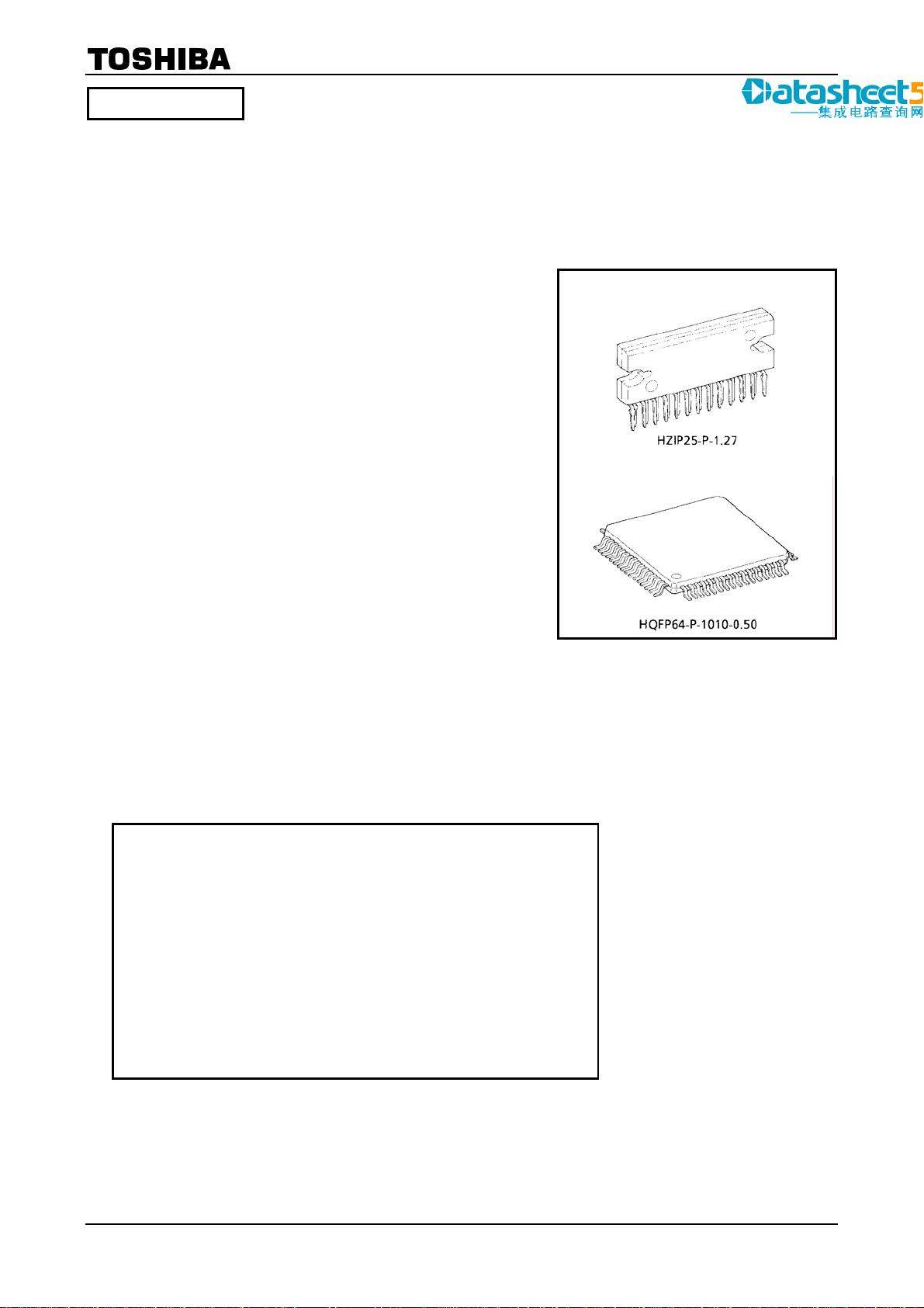
• Packages: HZIP25-P-1.27/HQFP64-P-1010-0.50
• Built-in input pull-down resistor: 100 kΩ (typ.)
• Output monitor pin equipped: MO current (I
MO
(max) = 1 mA)
• Equipped with reset and enable pins
• Built-in overheat protection circuit
*: Since this product has a MOS structure, it is sensitive to electrostatic discharge. These ICs are highly sensitive to
electrostatic discharge. When handling them, please be careful of electrostatic discharge, temperature and
humidity conditions.
TB6560HQ
TB6560FG
Weight:
HZIP25-P-1.27: 9.86 g (typ.)
HQFP64-P-1010-0.50: 0.26 g (typ.)
Preliminar
y
The TB6560HQ/FG is a Pb-free product.
The following conditions apply to solderability:
*Solderability
1. Use of Sn-63Pb solder bath
*solder bath temperature = 230°C
*dipping time = 5 seconds
*number of times = once
*use of R-type flux
2. Use of Sn-3.0Ag-0.5Cu solder bath
*solder bath temperature = 245°C
*dipping time = 5 seconds
*the number of times = once
*use of R-type flux
TB6560HQ/FG
2006-05-31
2
Block Diagram
M1
M2
CW/CCW
CLK
RESET
ENABLE
DCY1
DCY2
OSC
Input
circuit
OSC
V
DD
Maximum current
setting circuit
Current selector
circuit B
Overheat protection
circuit
Protect M
O
+
+
Bridge
driver A
Decode
r
V
MA
OUT_AP
OUT_AM
N
FA
V
MB
Bridge
driver B B
Decode
r
OUT_BP
OUT_BM
N
FB
TQ1 TQ2
SGND PGNDA PGNDB
Current selector
circuit A
10/1 1/42 2/43
11/2, 3, 4
9/61, 62
12/6, 7
8/55, 56
14/13, 14, 15
13/10, 11
16/19, 20
18/25, 26 17/2319/2820/30, 31
23/36
22/35
21/33
3/45
5/48
4/47
25/39
24/38
7/53
15/166/50, 51
TB6560HQ/TB6560FG
TB6560HQ/FG
2006-05-31
3
Pin Functions
Pin No.
HQ FG
I/O Symbol Functional Description
1 42 Input TQ2 Torque setting input (current setting) (built-in pull-down resistor)
2 43 Input TQ1
Torque setting input (current setting) (built-in pull-down resistor)
3 45 Input CLK Step transition, clock input (built-in pull-down resistor)
4 47 Input ENABLE H: Enable; L: All output OFF (built-in pull-down resistor)
5 48 Input
RESET
L: Reset (output is reset to its initial state) (built-in pull-down resistor)
6 50/51 ⎯ SGND Signal ground (control side) (Note 1)
7 53 ⎯ OSC Connects to and oscillates CR. Output chopping.
8 55/56 Input V
MB
Motor side power pin (B phase side) (Note 1)
9 61/62 Output OUT_BM OUT_B output (Note 1)
10 1 ⎯ PGNDB
Power ground
11 2/3/4 ⎯ N
FB
B channel output current detection pin (resistor connection).
Short the two pins for FG. (Note 1)
12 6/7 Output OUT_BP
OUT_B output (Note 1)
13 10/11 Output OUT_AM
OUT_A output (Note 1)
14 13/14/15 ⎯ N
FA
A channel output current detection pin (resistor connection).
Short the two pins for FG. (Note 1)
15 16 ⎯ PGNDA
Power ground
16 19/20 Output OUT_AP OUT_A output (Note 1)
17 23 Output M
O
Initial state detection output. ON when in initial state (open drain).
18 25/26 Input V
MA
Motor side power pin (A phase side) (Note 1)
19 28 Output Protect When TSD, ON (open drain). Normal Z.
20 30/31 Input V
DD
Control side power pin. (Note 1)
21 33 Input CW/CCW
Forward/Reverse toggle pin. L: Forward; H: Reverse
(built-in pull-down resistor)
22 35 Input M2 Excitation mode setting input (built-in pull-down resistor)
23 36 Input M1 Excitation mode setting input (built-in pull-down resistor)
24 38 Input DCY2 Current Decay mode setting input (built-in pull-down resistor)
25 39 Input DCY1 Current Decay mode setting input (built-in pull-down resistor)
HQ: No Non-connection (NC)
FG: Other than the above pins, all are NC
(Since NC pins are not connected to the internal circuit, a potential can be applied to those pins.)
All control input pins: Pull-down resistor 100 kΩ (typ.)
Note 1: If the FG pin number column indicates more than one pin, the indicated pins should be tied to each other at
a position as close to the pins as possible.
(The electrical characteristics of the relevant pins in this document refer to those when they are handled in
that way.)
<Terminal circuits>
Input pins
(M1, M2, CLK, CW/CCW,
ENABLE and RESET)
Output ins
(MO, PROTECT)
V
DD
100 kΩ
100 Ω
100 Ω
TB6560HQ/FG
2006-05-31
4
Absolute Maximum Ratings
(Ta
=
25°C)
Characteristic Symbol Rating Unit
V
DD
6
Power supply voltage
V
MA/B
40
V
HQ 3.5
Output current Peak
FG
I
O (PEAK)
2.5
A/phase
MO drain current I
(MO)
1 mA
Input voltage V
IN
5.5
V
5 (Note 1)
HQ
43 (Note 2)
1.7 (Note 3)
Power dissipation
FG
P
D
4.2 (Note 4)
W
Operating temperature T
opr
−30 to 85 °C
Storage temperature T
stg
−55 to 150 °C
Note 1: Ta = 25°C, No heat sink.
Note 2: Ta = 25°C, with infinite heat sink (HZIP25).
Note 3: Ta = 25°C, with soldered leads.
Note 4: Ta = 25°C, when mounted on the board (4-layer board).
Susceptible to the board layout and the mounting conditions.
Operating Range
(Ta
=
−
20 to 85°C)
Characteristic Symbol Test Condition Min Typ. Max Unit
V
DD
⎯ 4.5 5.0 5.5 V
Power supply voltage
V
MA/B
V
MA/B
>
=
V
DD
4.5 ⎯ 26.4 V
HQ ⎯ ⎯ ⎯ 3
Output current
FG
I
OUT
⎯ ⎯ 1.5
A
Input voltage V
IN
⎯ 0 ⎯ 5.5
V
Clock frequency f
CLK
⎯ ⎯ ⎯ 15 kHz
OSC frequency f
OSC
⎯ ⎯ ⎯ 600 kHz
TB6560HQ/FG
2006-05-31
5
Electrical Characteristics
(Ta
=
25°C, V
DD
=
5 V, V
M
=
24 V)
Characteristic Symbol
Test
Circuit
Test Condition Min Typ. Max Unit
High V
IN (H)
2.0 ⎯ V
DD
Input voltage
Low V
IN (L)
1
−0.2 ⎯ 0.8
V
Input hysteresis voltage V
H
1
M1, M2, CW/CCW, CLK,
RESET
,
ENABLE, DECAY, TQ1, TQ2, ISD
⎯ 400 ⎯ mV
I
IN (H)
M1, M2, CW/CCW, CLK, RESET ,
ENABLE, DECAY, TQ1, TQ2, ISD
V
IN
= 5.0 V
Built-in pull-down resistor
30 55 80
Input current
I
IN (L)
1
V
IN
= 0 V ⎯ ⎯ 1
µA
I
DD1
Output open,
RESET : H, ENABLE: H
(2, 1-2 phase excitation)
⎯ 3 5
I
DD2
Output open,
RESET : H, ENABLE: H
(W1−2, 2W1-2 phase excitation)
⎯ 3 5
I
DD3
RESET : L, ENABLE: L ⎯ 2 5
Consumption current V
DD
pin
I
DD4
1
RESET : H, ENABLE: L ⎯ 2 5
mA
I
M1
RESET : H/L, ENABLE: L ⎯ 0.5 1
Consumption current V
M
pin
I
M2
1
RESET : H/L, ENABLE: H ⎯ 0.7 2
mA
Output channel margin of error ∆V
O
⎯ B/A, C
OSC
= 0.0033 µF −5 ⎯ 5 %
V
NFHH
TQ1 = H, TQ2 = H 10 20 30
V
NFHL
TQ1 = L, TQ2 = H 47 50 55
V
NFLH
TQ1 = H, TQ2 = L 70 75 80
VNF level
Level differential
V
NFLL
⎯
TQ1
= L, TQ2 = L 100
%
Minimum clock pulse width t
W (CLK)
⎯ ⎯ ⎯ 100 ⎯ ns
MO output residual voltage V
OL
MO ⎯ I
OL
= 1 mA ⎯ ⎯ 0.5 V
TSD TSD ⎯ (Design target value) ⎯ 170 ⎯ °C
TSD hysteresis TSDhys ⎯ (Design target value) ⎯ 20 ⎯ °C
Oscillating frequency f
OSC
C = 330 pF 60 130 200 kHz
剩余31页未读,继续阅读
wxnlcyp_1
- 粉丝: 0
- 资源: 9
上传资源 快速赚钱
- 我的内容管理 收起
- 我的资源 快来上传第一个资源
- 我的收益 登录查看自己的收益
- 我的积分 登录查看自己的积分
- 我的C币 登录后查看C币余额
- 我的收藏
- 我的下载
- 下载帮助
会员权益专享
最新资源
- RTL8188FU-Linux-v5.7.4.2-36687.20200602.tar(20765).gz
- c++校园超市商品信息管理系统课程设计说明书(含源代码) (2).pdf
- 建筑供配电系统相关课件.pptx
- 企业管理规章制度及管理模式.doc
- vb打开摄像头.doc
- 云计算-可信计算中认证协议改进方案.pdf
- [详细完整版]单片机编程4.ppt
- c语言常用算法.pdf
- c++经典程序代码大全.pdf
- 单片机数字时钟资料.doc
- 11项目管理前沿1.0.pptx
- 基于ssm的“魅力”繁峙宣传网站的设计与实现论文.doc
- 智慧交通综合解决方案.pptx
- 建筑防潮设计-PowerPointPresentati.pptx
- SPC统计过程控制程序.pptx
- SPC统计方法基础知识.pptx
资源上传下载、课程学习等过程中有任何疑问或建议,欢迎提出宝贵意见哦~我们会及时处理!
点击此处反馈
安全验证
文档复制为VIP权益,开通VIP直接复制
信息提交成功
评论11