没有合适的资源?快使用搜索试试~ 我知道了~
首页AD7490 AD转换器
AD7490 AD转换器
4星 · 超过85%的资源 需积分: 49 48 下载量 71 浏览量
更新于2023-07-14
评论 1
收藏 2.21MB PDF 举报
AD7490是AD公司生产的一款A/D转换芯片。选用其28脚TSSOP封装形式的芯片。图5是其引脚功能图。从图5看出,共有VIN0—VIN1516路A/D通道,采样速率达1MHz,分辨率是12位。满足系统要求。量程为0— 或2 可通过写入寄存器实现,其中 可使用芯片AD780得到2.5V的稳定电压,利用调理电路实现量程转换以达到系统输入为±10V的要求。
资源详情
资源评论
资源推荐
a
Information furnished by Analog Devices is believed to be accurate and
reliable. However, no responsibility is assumed by Analog Devices for its
use, nor for any infringements of patents or other rights of third parties that
may result from its use. No license is granted by implication or otherwise
under any patent or patent rights of Analog Devices.
One Technology Way, P.O. Box 9106, Norwood, MA 02062-9106, U.S.A.
Tel: 781/329-4700 www.analog.com
Fax: 781/326-8703 © Analog Devices, Inc., 2002
REV. A
AD7490
16-Channel, 1 MSPS, 12-Bit ADC
with Sequencer in 28-Lead TSSOP
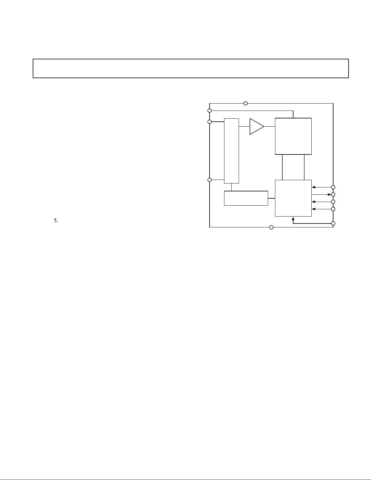
FUNCTIONAL BLOCK DIAGRAM
V
IN
0
•
•
•
•
•
•
•
•
•
•
•
•
•
V
IN
15
T/H
I/P
MUX
SEQUENCER
CONTROL LOGIC
12-BIT
SUCCESSIVE
APPROXIMATION
ADC
GND
SCLK
DOUT
DIN
CS
V
DRIVE
V
DD
AD7490
REF
IN
FEATURES
Fast Throughput Rate: 1 MSPS
Specified for V
DD
of 2.7 V to 5.25 V
Low Power at Max Throughput Rates:
5.4 mW Max at 870 kSPS with 3 V Supplies
12.5 mW Max at 1 MSPS with 5 V Supplies
16 (Single-Ended) Inputs with Sequencer
Wide Input Bandwidth:
69.5 dB SNR at 50 kHz Input Frequency
Flexible Power/Serial Clock Speed Management
No Pipeline Delays
High Speed Serial Interface SPI™/QSPI™/
MICROWIRE™/DSP Compatible
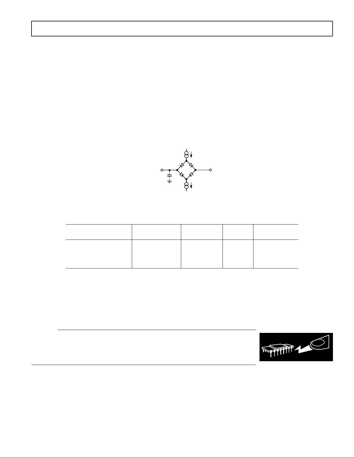
Full Shutdown Mode: 0.5 A Max
28-Lead TSSOP and 32-Lead LFCSP Packages
GENERAL DESCRIPTION
The AD7490 is a 12-bit high speed, low power, 16-channel,
successive-approximation ADC. The part operates from a single
2.7 V to 5.25 V power supply and features throughput rates up
to 1 MSPS. The part contains a low noise, wide bandwidth
track-and-hold amplifier that can handle input frequencies in
excess of 1 MHz.
The conversion process and data acquisition are controlled
using CS and the serial clock signal, allowing the device to
easily interface with microprocessors or DSPs. The input signal
is sampled on the falling edge of CS and conversion is also
initiated at this point. There are no pipeline delays associated
with the part.
The AD7490 uses advanced design techniques to achieve very
low power dissipation at high throughput rates. For maximum
throughput rates, the AD7490 consumes just 1.8 mA with 3 V
supplies, and 2.5 mA with 5 V supplies.
By setting the relevant bits in the Control Register, the analog
input range for the part can be selected to be a 0 to REF
IN
input or
a 0 to 2 REF
IN
with either straight binary or twos complement
output coding. The AD7490 features 16 single-ended analog
inputs with a channel sequencer to allow a preprogrammed
selection of channels to be converted sequentially.
The conversion time is determined by the SCLK frequency as
this is also used as the master clock to control the conversion.
The AD7490 is available in a 28-lead thin shrink small outline
(TSSOP) package, and a 32-lead chip scale package.
SPI and QSPI are trademarks of Motorola Inc.
MICROWIRE is a trademark of National Semiconductor Corporation
PRODUCT HIGHLIGHTS
1. High Throughput with Low Power Consumption
The AD7490 offers up to 1 MSPS throughput rates. At
maximum throughput with 3 V supplies, the AD7490
dissipates just 5.4 mW of power.
2. Sixteen Single-Ended Inputs with Channel Sequencer
A Sequence of channels can be selected, through which the
AD7490 will cycle and convert.
3. Single-Supply Operation with V
DRIVE
Function
The AD7490 operates from a single 2.7 V to 5.25 V supply.
The V
DRIVE
function allows the serial interface to connect
directly to either 3 V or 5 V processor systems independent
of V
DD
.
4. Flexible Power/Serial Clock Speed Management
The conversion rate is determined by the serial clock, allowing
the conversion time to be reduced through the serial clock
speed increase. The part also features various shutdown
modes to maximize power efficiency at lower throughput
rates. Power consumption is 0.5 µA max when in full shutdown.
5. No Pipeline Delay
The part features a standard successive-approximation ADC
with accurate control of the sampling instant via a CS input
and once off conversion control.
–2–
AD7490–SPECIFICATIONS
REV. A
(V
DD
= V
DRIVE
= 2.7 V to 5.25 V, REF
IN
= 2.5 V, f
SCLK
1
= 20 MHz, T
A
= T
MIN
to T
MAX
, unless
otherwise noted.)
Parameter B Version
2
Unit Test Conditions/Comments
DYNAMIC PERFORMANCE f
IN
= 50 kHz Sine Wave, f
SCLK
= 20 MHz
Signal to Noise +1 Distortion
(SINAD)
3
69 dB min @ 5 V, 70.5 dB typ
68 dB min @ 3 V, 69.5 dB typ
Signal to Noise Ratio (SNR)
3
69.5 dB min
Total Harmonic Distortion (THD)
3
–74 dB max @ 5 V, –84 dB typ
–71 dB max @ 3 V, –77 dB typ
Peak Harmonic or Spurious Noise (SFDR)
3
–75 dB max @ 5 V, –86 dB typ
–73 dB max @ 3 V, –80 dB typ
Intermodulation Distortion (IMD)
3
fa = 40.1 kHz, fb = 41.5 kHz
Second Order Terms –85 dB typ
Third Order Terms –85 dB typ
Aperture Delay 10 ns typ
Aperture Jitter 50 ps typ
Channel-to-Channel Isolation
3
–82 dB typ f
IN
= 400 kHz
Full Power Bandwidth 8.2 MHz typ @ 3 dB
1.6 MHz typ @ 0.1 dB
DC ACCURACY
3
Resolution 12 Bits
Integral Nonlinearity ±1 LSB max
Differential Nonlinearity –0.95/+1.5 LSB max Guaranteed No Missed Codes to 12 Bits
0V to V
REF IN
Input Range Straight Binary Output Coding
Offset Error ±8 LSB max ±0.6 LSB typ
Offset Error Match ±0.5 LSB max
Gain Error ±2 LSB max
Gain Error Match ±0.6 LSB max
0V to 2 V
REF IN
Input Range –V
REF IN
to +V
REF IN
Biased about V
REF
with
Twos Complement Output Coding Offset
Positive Gain Error ±2 LSB max
Positive Gain Error Match ±0.5 LSB max
Zero Code Error ±8 LSB max ±0.6 LSB typ
Zero Code Error Match ±0.5 LSB max
Negative Gain Error ±1 LSB max
Negative Gain Error Match ±0.5 LSB max
ANALOG INPUT
Input Voltage Ranges 0 to REF
IN
V RANGE Bit Set to 1
0 to 2 REF
IN
V RANGE Bit Set to 0,
V
DD
/V
DRIVE
= 4.75 V to 5.25 V for 0 to 2 REF
IN
DC Leakage Current ±1 µA max
Input Capacitance 20 pF typ
REFERENCE INPUT
REF
IN
Input Voltage 2.5 V ±1% Specified Performance
DC Leakage Current ±1 µA max
REF
IN
Input Impedance 36 kΩ typ f
SAMPLE
= 1 MSPS
LOGIC INPUTS
Input High Voltage, V
INH
0.7 V
DRIVE
V min
Input Low Voltage, V
INL
0.3 V
DRIVE
V max
Input Current, I
IN
±1 µA max Typically 10 nA, V
IN
5 0 V or V
DRIVE
Input Capacitance, C
IN
4
10 pF max
LOGIC OUTPUTS
Output High Voltage, V
OH
V
DRIVE
– 0.2 V min I
SOURCE
= 200 µA; V
DD
= 2.7 V to 5.25 V
Output Low Voltage, V
OL
0.4 V max I
SINK
= 200 µA
Floating-State Leakage Current ±10 µA max Weak/Tri Bit Set to 0
Floating-State Output Capacitance
4
10 pF max Weak/Tri Bit Set to 0
Output Coding Straight (Natural) Binary Coding Bit Set to 1
Twos Complement Coding Bit Set to 0
AD7490
–3–REV. A
Parameter B Version
2
Unit Test Conditions/Comments
CONVERSION RATE
Conversion Time 800 ns max 16 SCLK Cycles, SCLK = 20 MHz
Track-and-Hold Acquisition Time
3
300 ns max Sine Wave Input
300 ns max Full-Scale Step Input
Throughput Rate 1 MSPS max @ 5 V (See Serial Interface section.)
POWER REQUIREMENTS
V
DD
2.7/5.25 V min/max
V
DRIVE
2.7/5.25 V min/max
I
DD
5
Digital I/Ps = 0 V or V
DRIVE
Normal Mode (Static) 600 µA typ V
DD
= 2.7 V to 5.25 V, SCLK On or Off
Normal Mode (Operational) 2.5 mA max V
DD
= 4.75 V to 5.25 V, f
SCLK
= 20 MHz
(f
S
= Max Throughput) 1.8 mA max V
DD
= 2.7 V to 3.6 V, f
SCLK
= 20 MHz
Auto Standby Mode 1.55 mA typ f
SAMPLE
= 500 kSPS
92 µA max Static
Auto Shutdown Mode 960 µA typ f
SAMPLE
= 250 kSPS
0.5 µA max Static
Full Shutdown Mode 0.5 µA max SCLK On or Off (20 nA typ)
Power Dissipation
5
Normal Mode (Operational) 12.5 mW max V
DD
= 5 V, f
SCLK
= 20 MHz
5.4 mW max V
DD
= 3 V, f
SCLK
= 20 MHz
Auto Standby Mode (Static) 460 µW max V
DD
= 5 V
276 µW max V
DD
= 3 V
Auto Shutdown Mode (Static) 2.5 µW max V
DD
= 5 V
1.5 µW max V
DD
= 3 V
Full Shutdown Mode 2.5 µW max V
DD
= 5 V
1.5 µW max V
DD
= 3 V
NOTES
1
Specifications apply for f
SCLK
up to 20 MHz. However, for serial interfacing requirements, see Timing Specifications.
2
Temperature Ranges (B Version): –40°C to +85°C.
3
See Terminology section.
4
Sample tested at 25°C to ensure compliance.
5
See Power Versus Throughput Rate section.
Specifications subject to change without notice.
–4–
AD7490
REV. A
TIMING SPECIFICATIONS
1
Limit at T
MIN
, T
MAX
Parameter V
DD
= 3 V V
DD
= 5 V Unit Description
f
SCLK
2
10 10 kHz min
16 20 MHz max
t
CONVERT
16 t
SCLK
16 t
SCLK
t
QUIET
50 50 ns min Minimum Quiet Time Required between Bus
Relinquish and Start of Next Conversion
t
2
12 10 ns min CS to SCLK Setup Time
t
3
3
20 14 ns max Delay from CS until DOUT Three-State Disabled
t
3
b
4
30 20 ns max Delay from CS to DOUT Valid
t
4
3
60 40 ns max Data Access Time after SCLK Falling Edge
t
5
0.4 t
SCLK
0.4 t
SCLK
ns min SCLK Low Pulsewidth
t
6
0.4 t
SCLK
0.4 t
SCLK
ns min SCLK High Pulsewidth
t
7
15 15 ns min SCLK to DOUT Valid Hold Time
t
8
5
15/50 15/50 ns min/max SCLK Falling Edge to DOUT High Impedance
t
9
20 20 ns min DIN Setup Time prior to SCLK Falling Edge
t
10
55ns min DIN Hold Time after SCLK Falling Edge
t
11
20 20 ns min Sixteenth SCLK Falling Edge to CS High
t
12
11µs max Power-Up Time from Full Power-Down/
Auto Shutdown/Auto Standby Modes
NOTES
1
Sample tested at 25°C to ensure compliance. All input signals are specified with tr = tf = 5 ns (10% to 90% of V
DD
) and timed from a voltage level of 1.6 V.
(See Figure 1.) The 3 V operating range spans from 2.7 V to 3.6 V. The 5 V operating range spans from 4.75 V to 5.25 V.
2
Mark/Space ratio for the SCLK input is 40/60 to 60/40. The maximum SCLK frequency is 16 MHz with V
DD
= 3 V to give a throughput of 870 kSPS. Care must be
taken when interfacing to account for data access time t
4
, and the setup time required for the user’s processor. These two times will determine the maximum SCLK
frequency with which the user’s system can operate. (See Serial Interface section.)
3
Measured with the load circuit of Figure 1 and defined as the time required for the output to cross 0.4 V or 0.7 V
DRIVE
V.
4
t
3
b represents a worst-case figure for having ADD3 available on the DOUT line, i.e., if the AD7490 went back into three-state at the end of a conversion and some
other device took control of the bus between conversions, the user would have to wait a maximum time of t
3
b before having ADD3 valid on DOUT line. If the DOUT
line is weakly driven to ADD3 between conversions, then the user would typically have to wait 17 ns at 3 V and 12 ns at 5 V after the CS falling edge before seeing
ADD3 valid on DOUT.
5
t
8
is derived from the measured time taken by the data outputs to change 0.5 V when loaded with the circuit of Figure 1. The measured number is then extrapolated
back to remove the effects of charging or discharging the 25 pF capacitor. This means that the time, t
8
, quoted in the timing characteristics, is the true bus relinquish
time of the part and is independent of the bus loading.
Specifications subject to change without notice.
(V
DD
= 2.7 V to 5.25 V, V
DRIVE
≤
V
DD
, REF
IN
= 2.5 V; T
A
= T
MIN
to T
MAX
, unless otherwise noted.)
AD7490
–5–REV. A
ABSOLUTE MAXIMUM RATINGS
1
(T
A
= 25°C, unless otherwise noted.)
V
DD
to GND . . . . . . . . . . . . . . . . . . . . . . . . . . –0.3 V to +7 V
V
DRIVE
to GND . . . . . . . . . . . . . . . . . . –0.3 V to V
DD
+ 0.3 V
Analog Input Voltage to GND . . . . . . . –0.3 V to V
DD
+ 0.3 V
Digital Input Voltage to GND . . . . . . . . . . . . . –0.3 V to +7 V
Digital Output Voltage to GND . . . . . –0.3 V to V
DD
+ 0.3 V
REF
IN
to GND . . . . . . . . . . . . . . . . . . –0.3 V to V
DD
+ 0.3 V
Input Current to Any Pin Except Supplies
2
. . . . . . . . ±10 mA
Operating Temperature Ranges
Commercial (B Version) . . . . . . . . . . . . . . –40°C to +85°C
Storage Temperature Range . . . . . . . . . . . –65°C to +150°C
Junction Temperature . . . . . . . . . . . . . . . . . . . . . . . . . . 150°C
I
OL
I
OH
1.6V
TO
OUTPUT
PIN
C
L
25pF
200A
200A
Figure 1. Load Circuit for Digital Output Timing Specifications
LFCSP, TSSOP Package, Power Dissipation . . . . . . 450 mW
θ
JA
Thermal Impedance . . . . . . . . . . . 108.2°C/W (LFCSP)
. . . . . . . . . . . . . . . . . . . . . . . . . . . . 97.9°C/W (TSSOP)
θ
JC
Thermal Impedance . . . . . . . . . . . 32.71°C/W (LFCSP)
. . . . . . . . . . . . . . . . . . . . . . . . . . . . . . 14°C/W (TSSOP)
Lead Temperature, Soldering
Vapor Phase (60 sec) . . . . . . . . . . . . . . . . . . . . . . 215°C
Infrared (15 sec) . . . . . . . . . . . . . . . . . . . . . . . . . 220°C
ESD . . . . . . . . . . . . . . . . . . . . . . . . . . . . . . . . . . . . . . . . 1 kV
NOTES
1
Stresses above those listed under Absolute Maximum Ratings may cause perma-
nent damage to the device. This is a stress rating only; functional operation of the
device at these or any other conditions above those listed in the operational
sections of this specification is not implied. Exposure to absolute maximum rating
conditions for extended periods may affect device reliability.
2
Transient currents of up to 100 mA will not cause SCR latch up.
ORDERING GUIDE
Temperature Linearity Package Package
Model Range Error (LSB)
1
Option Description
AD7490BCP –40°C to +85°C ±1 CP-32 LFCSP
AD7490BRU –40°C to +85°C ±1 RU-28 TSSOP
EVAL-AD7490CB
2
Evaluation Board
EVAL-CONTROL BRD2
3
Controller Board
NOTES
1
Linearity error refers to integral linearity error.
2
This can be used as a stand-alone evaluation board or in conjunction with the Evaluation Controller Board for evaluation/
demonstration purposes.
3
This board is a complete unit allowing a PC to control and communicate with all Analog Devices evaluation boards ending in
the CB designators. To order a complete evaluation kit, you will need to order the particular ADC evaluation board, e.g.,
EVAL-AD7490CB, the EVAL-CONTROL-BRD2, and a 12 V ac transformer. See relevant evaluation board technical note for
more information.
CAUTION
ESD (electrostatic discharge) sensitive device. Electrostatic charges as high as 4000 V readily
accumulate on the human body and test equipment and can discharge without detection. Although
the AD7490 features proprietary ESD protection circuitry, permanent damage may occur on
devices subjected to high energy electrostatic discharges. Therefore, proper ESD precautions are
recommended to avoid performance degradation or loss of functionality.
WARNING!
ESD SENSITIVE DEVICE
剩余23页未读,继续阅读
lifangnuaa
- 粉丝: 2
- 资源: 2
上传资源 快速赚钱
- 我的内容管理 收起
- 我的资源 快来上传第一个资源
- 我的收益 登录查看自己的收益
- 我的积分 登录查看自己的积分
- 我的C币 登录后查看C币余额
- 我的收藏
- 我的下载
- 下载帮助
会员权益专享
最新资源
- zigbee-cluster-library-specification
- JSBSim Reference Manual
- c++校园超市商品信息管理系统课程设计说明书(含源代码) (2).pdf
- 建筑供配电系统相关课件.pptx
- 企业管理规章制度及管理模式.doc
- vb打开摄像头.doc
- 云计算-可信计算中认证协议改进方案.pdf
- [详细完整版]单片机编程4.ppt
- c语言常用算法.pdf
- c++经典程序代码大全.pdf
- 单片机数字时钟资料.doc
- 11项目管理前沿1.0.pptx
- 基于ssm的“魅力”繁峙宣传网站的设计与实现论文.doc
- 智慧交通综合解决方案.pptx
- 建筑防潮设计-PowerPointPresentati.pptx
- SPC统计过程控制程序.pptx
资源上传下载、课程学习等过程中有任何疑问或建议,欢迎提出宝贵意见哦~我们会及时处理!
点击此处反馈
安全验证
文档复制为VIP权益,开通VIP直接复制
信息提交成功
评论6