
Dual Automotive DSI3 Master Transceiver E521.42
PRODUCTION DATA – Apr 04, 2022
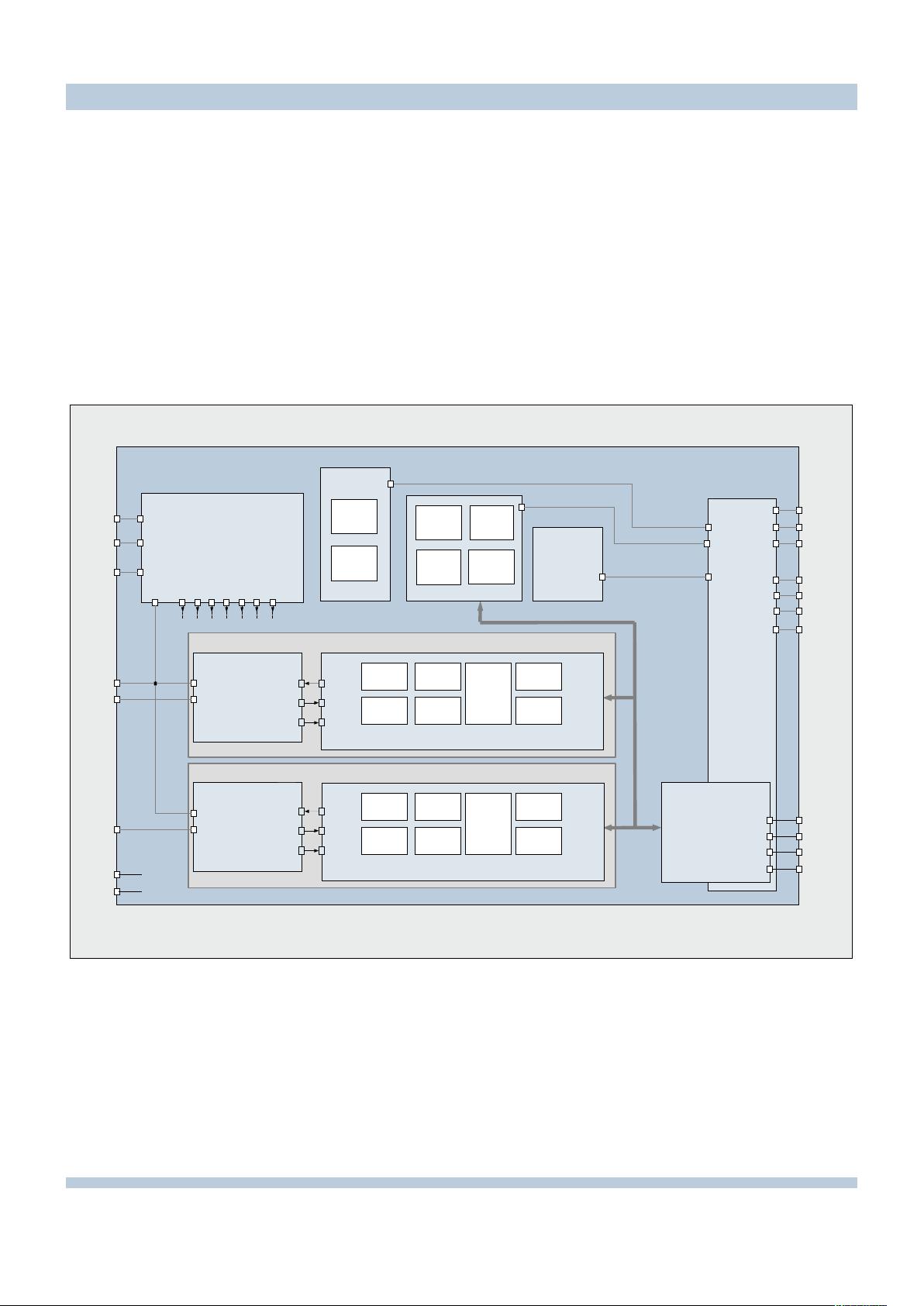
7 Functional Description
7.1 Overview
The DSI3 master IC realizes data communication consisting of
• a SPI interface for ECU host communication,
• two DSI data channels with data buffers and
• two DSI physical transceivers
The main control block implements common functionality used for overall circuit and communication control.
The supply and references block contains all necessary analog functional blocks to provide internally regulated
supply voltages, reference currents and supervise supply voltage levels (external and internal).
Supplies and References - SUP
VBAT
VCC
VDD18
Main Control
VDD18
OTP Test
System
Status
Main
FSM
INTN_C
DSI3
Physical Layer
TXD
RXD
ERROR
DSI Digital Part
Transmit
Coder
Protocol
Decoder
Threshold
Adap#on
Error
Handling
Data Bu'er
Channel
FSM
Time
Control
BUS_CH[]
DSI3 Interface
DSI3
Physical Layer
BUS_SPI[]
DSI Digital Part
Transmit
Coder
Protocol
Decoder
Threshold
Adap#on
Error
Handling
Data Bu'er
Channel
FSM
Time
Control
BUS_CH[]
TXD
RXD
ERROR
CLKREF
RESB
VDSI
DSI1
DSI2
VREF[]
IBIAS[]
ICONST[]
CLK
POR
BGREF
UV
VCC
GND
DGND
DSI3 Interface
Digital
IOs
Timebase
PLL
CLKREF
supervision
Interrupt System
INTB
VIO
CLKREF
RESB
INTB
DCR1B
DCR2B
RFC
Serial
Peripheral
Interface
SPI
BUS_SPI[]
MISO_SPI
MOSI_SPI
SCK_SPI
CSB_SPI
MISO
MOSI
SCK
CSB
VDSI
VBAT
Figure 7.1-1: Detailed Block Diagram (Subblocks, standard functions)
All individual register addresses are calculated from a base address (see following table) and an individual address
offset (see register tables of data sheet chapters).
ELMOS Semiconductor SE reserves the right to change the detail specifications as may be required to permit improvements in the design of its products.
Elmos Semiconductor SE
Data Sheet
25DS0056E.07
14 / 82

剩余81页未读,继续阅读


