7.6 Electrical Characteristics: Power Consumption
typical values at T
A
= 25°C, VA19 = 1.9 V, VPLL19 = 1.9 V, VREFO = 1.9 V, VTRIG = 1.1V, VA11 = 1.1 V, VD11 = 1.1
V, default full-scale voltage (V
FS
= 0.8 V
PP
), f
IN
= 97 MHz, A
IN
= –1 dBFS, f
CLK
= 800 MHz, filtered 1 V
PP
sine-wave clock
applied to CLK±, PLL disabled, JMODE = 0, High Performance Mode and foreground calibration (unless otherwise noted);
minimum and maximum values are at nominal supply voltages and over the operating free-air temperature range provided in
the Recommended Operating Conditions table
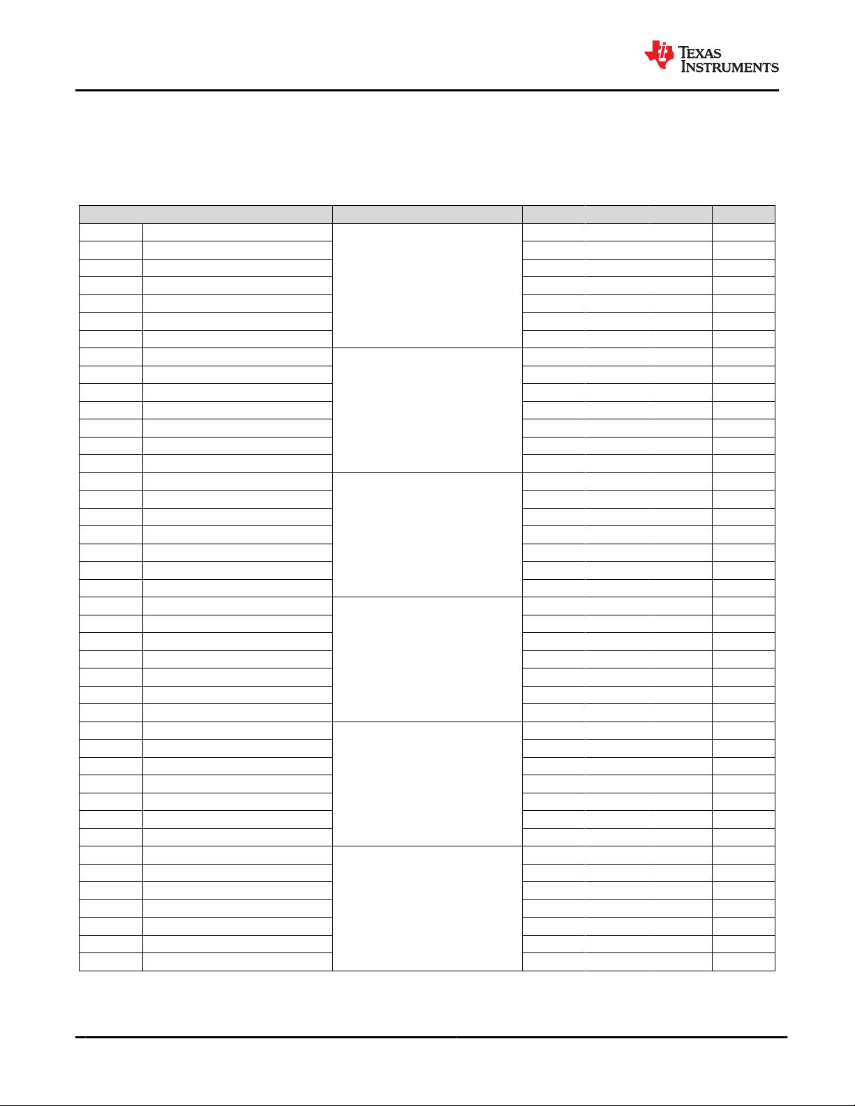
PARAMETER TEST CONDITIONS MIN TYP MAX UNIT
I
VA19
1.9-V analog supply current
Power mode 1a: Quad channel, JMODE
0 (12-bit, 8 lanes, 8B/10B encoding), FG
calibration, PLL_EN = 0, f
S
= 0.8 GSPS,
High Performance Mode
655 mA
I
VPLL19
PLL analog supply current 0 mA
I
VREFO
PLLREFO± analog supply current 0 mA
I
VTRIG
TRIGOUT± analog supply current 0 mA
I
VA11
1.1-V analog supply current 465 mA
I
VD11
1.1-V digital supply current 395 mA
P
DIS
Power dissipation 2.18 W
I
VA19
1.9-V analog supply current
Power mode 1b: Dual channel, JMODE
0 (12-bit, 4 lanes, 8B/10B encoding), FG
calibration, PLL_EN = 0,0.8 GSPS, High
Performance Mode
390 mA
I
VPLL19
PLL analog supply current 0 mA
I
VREFO
PLLREFO± analog supply current 0 mA
I
VTRIG
TRIGOUT± analog supply current 0 mA
I
VA11
1.1-V analog supply current 350 mA
I
VD11
1.1-V digital supply current 250 mA
P
DIS
Power dissipation 1.41 W
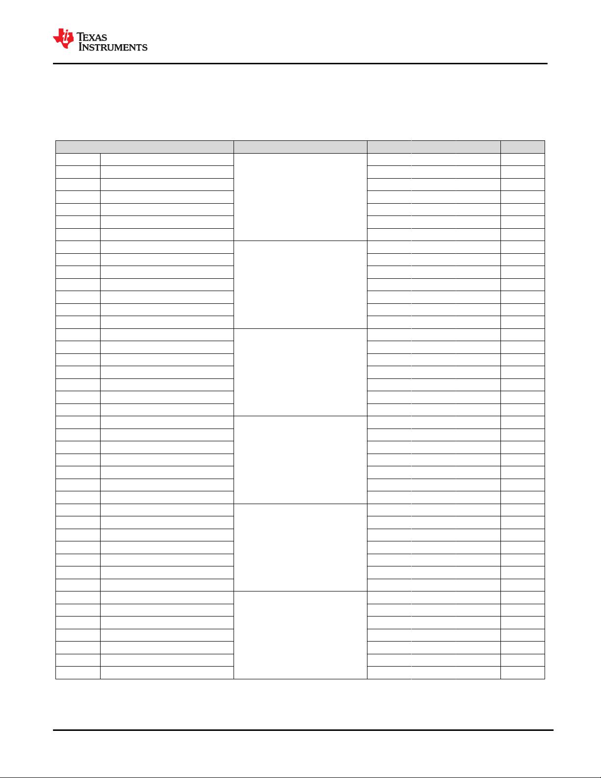
I
VA19
1.9-V analog supply current
Power mode 1c: Single channel, JMODE
0 (12-bit, 2 lanes, 8B/10B encoding), FG
calibration, PLL_EN = 0, f
S
= 0.8 GSPS,
High Performance Mode
253 mA
I
VPLL19
PLL analog supply current 0 mA
I
VREFO
PLLREFO± analog supply current 0 mA
I
VTRIG
TRIGOUT± analog supply current 0 mA
I
VA11
1.1-V analog supply current 316 mA
I
VD11
1.1-V digital supply current 160 mA
P
DIS
Power dissipation 1.01 W
I
VA19
1.9-V analog supply current
Power mode 2a: Quad channel, JMODE
8 (12-bit, 4 lanes, 64B/66B encoding),
LPBG calibration, PLL_EN = 0, f
S
= 0.8
GSPS, Low Power Mode
565 mA
I
VPLL19
PLL analog supply current 0 mA
I
VREFO
PLLREFO± analog supply current 0 mA
I
VTRIG
TRIGOUT± analog supply current 0 mA
I
VA11
1.1-V analog supply current 355 mA
I
VD11
1.1-V digital supply current 330 mA
P
DIS
Power dissipation 1.83
(1)
W
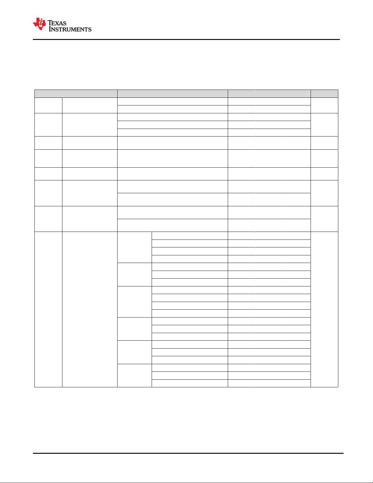
I
VA19
1.9-V analog supply current
Power mode 2b: Dual channel, JMODE
8 (12-bit, 2 lanes, 64B/66B encoding),
LPBG calibration, PLL_EN = 0, f
S
= 0.8
GSPS, Low Power Mode
345 mA
I
VPLL19
PLL analog supply current 0 mA
I
VREFO
PLLREFO± analog supply current 0 mA
I
VTRIG
TRIGOUT± analog supply current 0 mA
I
VA11
1.1-V analog supply current 306 mA
I
VD11
1.1-V digital supply current 198 mA
P
DIS
Power dissipation 1.19
(1)
W
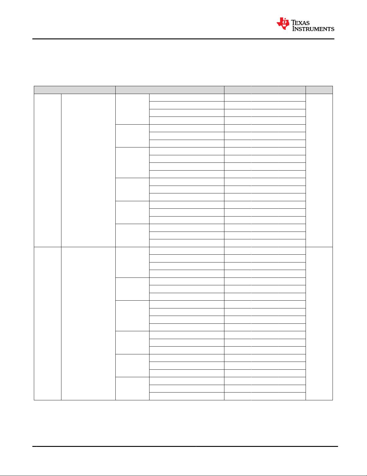
I
VA19
1.9-V analog supply current
Power mode 2c: Single channel, JMODE
8 (12-bit, 1 lanes, 64B/66B encoding),
LPBG calibration, PLL_EN = 0, f
S
= 0.8
GSPS, Low Power Mode
235 mA
I
VPLL19
PLL analog supply current 0 mA
I
VREFO
PLLREFO± analog supply current 0 mA
I
VTRIG
TRIGOUT± analog supply current 0 mA
I
VA11
1.1-V analog supply current 283 mA
I
VD11
1.1-V digital supply current 146 mA
P
DIS
Power dissipation 0.92
(1)
W
ADC12QJ800-Q1, ADC12DJ800-Q1, ADC12SJ800-Q1
SBASA52 – JULY 2021
www.ti.com
16 Submit Document Feedback
Copyright © 2021 Texas Instruments Incorporated
Product Folder Links: ADC12QJ800-Q1 ADC12DJ800-Q1 ADC12SJ800-Q1
