
TLP2768A
5
10.
10.
10.
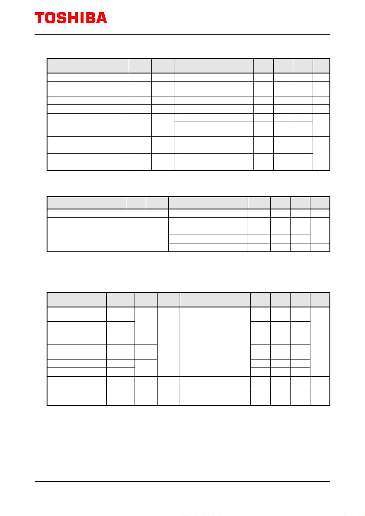
10. Electrical Characteristics (Note)
Electrical Characteristics (Note)
Electrical Characteristics (Note)
Electrical Characteristics (Note)
(Unless otherwise specified, T
(Unless otherwise specified, T
(Unless otherwise specified, T
(Unless otherwise specified, T
a
a
a
a
= -40 to 125
= -40 to 125
= -40 to 125
= -40 to 125
, V
, V
, V
, V
CC
CC
CC
CC
= 2.7 to 5.5 V)
= 2.7 to 5.5 V)
= 2.7 to 5.5 V)
= 2.7 to 5.5 V)
Characteristics
Input forward voltage
Input forward voltage temperature
coefficient
Input reverse current
Input capacitance
High-level output current
Low-level output voltage
High-level supply current
Low-level supply current
Threshold input current (H/L)
Symbol
V
F
∆V
F
/∆T
a
I
R
C
t
I
OH
V
OL
I
CCH
I
CCL
I
FHL
Test
Circuit
Fig.13.1.1
Fig.13.1.2
Fig.13.1.3
Fig.13.1.4
Test Condition
I
F
= 10 mA, T
a
= 25
I
F
= 10 mA
V
R
= 5 V, T
a
= 25
V
S
= 0 V, f = 1 MHz, T
a
= 25
V
CC
= V
O
= 5.5 V, V
F
= 0.8 V
V
CC
= V
O
= 5.5 V, V
F
= 0.8 V,
T
a
= 25
I
F
= 10 mA, I
O
= 13 mA
I
F
= 0 mA
I
F
= 10 mA
I
O
= 13 mA, V
O
< 0.6 V
Min
1.45
Typ.
1.55
-2.0
20
Max
1.70
10
50
10
0.6
4
4
5.0
Unit
V
mV/
µA
pF
µA
V
mA
Note: All typical values are at T
a
= 25 .
11.
11.
11.
11. Isolation Characteristics (Unless otherwise specified, T
Isolation Characteristics (Unless otherwise specified, T
Isolation Characteristics (Unless otherwise specified, T
Isolation Characteristics (Unless otherwise specified, T
a
a
a
a
= 25
= 25
= 25
= 25
)
)
)
)
Characteristics
Total capacitance (input to output)
Isolation resistance
Isolation voltage
Symbol
C
S
R
S
BV
S
Note
(Note 1)
(Note 1)
(Note 1)
Test Condition
V
S
= 0 V, f = 1 MHz
V
S
= 500 V, R.H. ≤ 60 %
AC, 60 s
AC, 1 s in oil
DC, 60 s in oil
Min
1 × 10
12
5000
Typ.
1.0
10
14
10000
10000
Max
Unit
pF
Ω
Vrms
Vdc
Note 1: This device is considered as a two-terminal device: Pins 1, 2 and 3 are shorted together, and pins 4, 5 and 6
are shorted together.
12.
12.
12.
12. Switching Characteristics (Note)
Switching Characteristics (Note)
Switching Characteristics (Note)
Switching Characteristics (Note)
(Unless otherwise specified, T
(Unless otherwise specified, T
(Unless otherwise specified, T
(Unless otherwise specified, T
a
a
a
a
= -40 to 125
= -40 to 125
= -40 to 125
= -40 to 125
, V
, V
, V
, V
CC
CC
CC
CC
= 2.7 to 5.5 V)
= 2.7 to 5.5 V)
= 2.7 to 5.5 V)
= 2.7 to 5.5 V)
Characteristics
Propagation delay time
(H/L)
Propagation delay time
(L/H)
Pulse width distortion
Propagation delay skew
(device to device)
Fall time
Rise time
Common-mode transient
immunity at output high
Common-mode transient
immunity at output low
Symbol
t
pHL
t
pLH
|t
pHL
-t
pLH
|
t
psk
t
f
t
r
CM
H
CM
L
Note
(Note 1)
(Note 1),
(Note 2)
(Note 1)
Test
Circuit
Fig.13.1.5
Fig.13.1.6
Test Condition
I
F
= 7.5 mA, C
L
= 15 pF,
R
L
= 350 Ω
I
F
= 0 mA, V
CC
= 5 V,
V
CM
= 1000 V
p-p
, T
a
= 25
I
F
= 10 mA, V
CC
= 5 V,
V
CM
= 1000 V
p-p
, T
a
= 25
Min
-40
±20
±20
Typ.
30
30
±25
±25
Max
60
60
35
40
Unit
ns
kV/µs
Note: All typical values are at T
a
= 25 .
Note 1: f = 5 MHz, duty = 50 %, input current t
r
= t
f
= 5 ns, C
L
is approximately 15 pF which includes probe and stray
wiring capacitance.
Note 2: The propagation delay skew, t
psk
, is equal to the magnitude of the worst-case difference in t
pHL
and/or t
pLH
that will be seen between units at the same given conditions (supply voltage, input current, temperature, etc).
2017-12-26
Rev.9.0
©2015-2017
Toshiba Electronic Devices & Storage Corporation
剩余20页未读,继续阅读

auiyn
- 粉丝: 3
- 资源: 106
 我的内容管理
展开
我的内容管理
展开


最新资源
- C++多态实现机制详解:虚函数与早期绑定
- Java多线程与异常处理详解
- 校园导游系统:无向图实现最短路径探索
- SQL2005彻底删除指南:避免重装失败
- GTD时间管理法:提升效率与组织生活的关键
- Python进制转换全攻略:从10进制到16进制
- 商丘物流业区位优势探究:发展战略与机遇
- C语言实训:简单计算器程序设计
- Oracle SQL命令大全:用户管理、权限操作与查询
- Struts2配置详解与示例
- C#编程规范与最佳实践
- C语言面试常见问题解析
- 超声波测距技术详解:电路与程序设计
- 反激开关电源设计:UC3844与TL431优化稳压
- Cisco路由器配置全攻略
- SQLServer 2005 CTE递归教程:创建员工层级结构
资源上传下载、课程学习等过程中有任何疑问或建议,欢迎提出宝贵意见哦~我们会及时处理!
点击此处反馈


