182 Vanish and Toumazou
feedback is applied from the collector of Q3 to the in-
put via
Rf. The purpose of the common-base input
transistor is to significantly reduce the input resistance
of the preamplifier so that photodiode capacitance is
virtually insignificant in determinng the bandwidth of
the amplifier. Furthermore due to the low input
resistance of the common-base, current feedback can
now be applied offering the high gain-bandwidth poten-
tial associated with the feedback [6]. The purpose of
including a second gain stage is to provide phase in-
version and also increase the open-loop transimpedance
gain of the amplifier so that when current feedback is
applied,
Rf can be made large with no significant
penalty in bandwidth [4, 5].
3. Low-Noise Common-Base Architecture
Despite the advantages of the common-base circuit of
figure lc the common-base transistor has unity current
gain and so all noise contributions from common-base
load resistance
R a and common-collector transistor Q2
are transferred directly to the input.' R a now con-
tributes to the noise performance and so for noise
reduction Ra should be made as large as possible.
However, since Rr also dictates the open-loop pole
locations of the amplifier then for large values of R 4
the nondominant pole frequency reduces to some ex-
tent, leading to potential instability. To overcome this
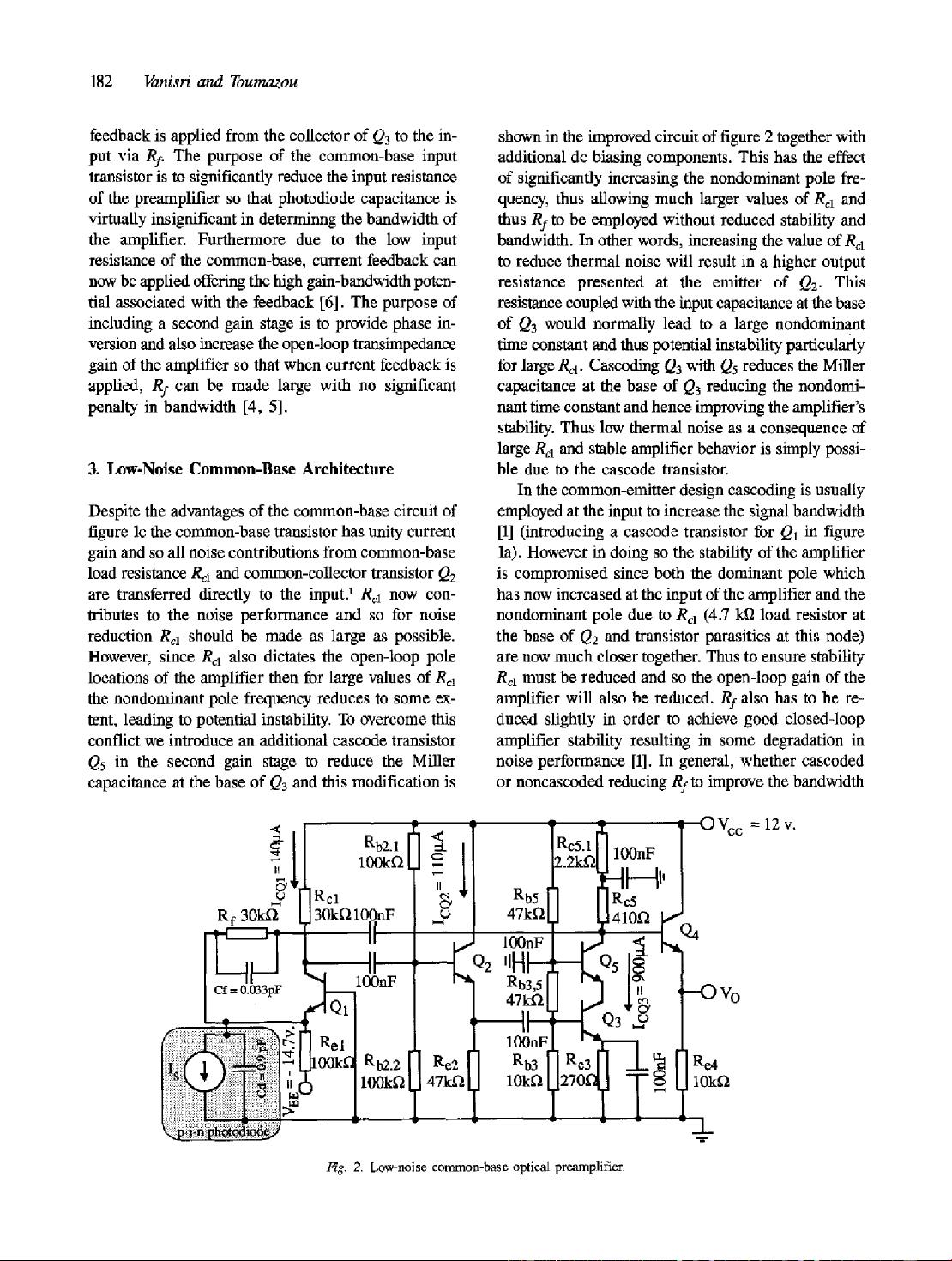
conflict we introduce an additional cascode transistor
(25 in the second gain stage to reduce the Miller
capacitance at the base of Q3 and this modification is
shown in the improved circuit of figure 2 together with
additional dc biasing components. This has the effect
of significantly increasing the nondominant pole fre-
quency, thus allowing much larger values of Ra and
thus
Ry to be employed without reduced stability and
bandwidth. In other words, increasing the value of Ra
to reduce thermal noise will result in a higher output
resistance presented at the emitter of Q2- This
resistance coupled with the input capacitance at the base
of Q3 would normally lead to a large nondominant
time constant and thus potential instability particularly
for large
Rcl. Cascoding Q3 with Q5 reduces the Miller
capacitance at the base of Q3 reducing the nondomi-
nant time constant and hence improving the amplifier's
stability. Thus low thermal noise as a consequence of
large
R a and stable amplifier behavior is simply possi-
ble due to the cascode transistor.
In the common-emitter design cascoding is usually
employed at the input to increase the signal bandwidth
[1] (introducing a cascode transistor for Q1 in figure
la). However in doing so the stability of the amplifier
is compromised since both the dominant pole which
has now increased at the input of the amplifier and the
nondominant pole due to Re1 (4.7 kl2 load resistor at
the base of Q2 and transistor parasitics at this node)
are now much closer together. Thus to ensure stability
Rr must be reduced and so the open-loop gain of the
amplifier will also be reduced.
Rf also has to be re-
duced slightly in order to achieve good closed-loop
amplifier stability resulting in some degradation in
noise performance [1]. In general, whether cascoded
or noncascoded reducing
Rf to improve the bandwidth
I
] Rb2.1
f3o .1o .
............................
:::::::::::::::::::::: :::::: :':::::::: [~ l
i@::!
i ~, i OVcc =
12
v.
/RcS"l I I 100nF /
'b, [1 [1Rc5 /
I~;F~ d41~ ~Q4
t :h 18
b
Rb3,511
'"1 --O v.
47k-~11 t.~ ,I,~ u
~ -- l
Fig. 2. Low-noise common-base optical preamplifier.


