628
IEEE
TRANSACTIONS
ON
COMPONENTS,
HYBRIDS,
AND
MANUFACTURING
TECHNOLOGY,
VOL.
16,
NO.
7,
NOVEMBER
1993
and
B
and the destination of data in either RAM A or
B.
The read-modify-write cycle is limited to single sources and
destinations in RAM A and
B
and the RAM address may
not be changed during an operation. If a different destination
address is required, or if source addresses in the same RAM
are required, additional clock cycles are necessary. However,
this is
not
a significant performance limitation since it is rare
in practice to require this type of operation.
4)
Multiplexers:
The
5
multiplexers control the selection
of input data to the addedsubtractor, RAM’s
A
and
B,
a
vertical communications register (CM) and a no-op signal
(FG). Command bit combinations which are out of range
will result
in
no input selection and the latches following the
multiplexer will then retain the previous data.
5)
Latches:
The latches store the output data from five of
the multiplexers, three of them (NS, EW, C) hold inputs to the
adder/subtractor, one (CM) forms part of a communication
register and the fifth (FLG) is a conditional flag store. All
latches are
full
clock cycle delay latches. However, an output
is fed from the NS, EW, and C latches to the ALU in the first
half
of the clock cycle
so
that the
ALU
output is available
to be written to the RAM’s during the second half of the
cycle. The output from the FLG latch is used to produce a
conditional flag signal FG
=
not
C2
+
FLG, where
C2
is
a global command input. When FLG is low, all the latches,
except CM, are inhibited from receiving new data and retain
their previous state. This has the effect of halting operation of
the PE
so
that local conditionals can be executed. The FLG
register can be set either as a result of an arithmetic operation
or by a simple memory fetch. By initializing the memories
of the PE’s in groups, isolated areas of the array can execute
different programs. This feature can be used to form arbitrary
arrays of processors under software control.
6)
AdderISubtractor:
The adderlsubtractor has inputs A,
B,
CIN, and outputs SM, CY, where CIN and CY are the
carry/borrow signals. The adderlsubtractor can perform the
usual arithmetic and logical functions by appropriate setting
of the inputs and can be programmed to perform (A-B-CIN)
and (B-A-CIN).
The global output signal is
a wired-OR output that is pulled low by any PE for which FG
is high and
C
is low.
8)
The Array Structure:
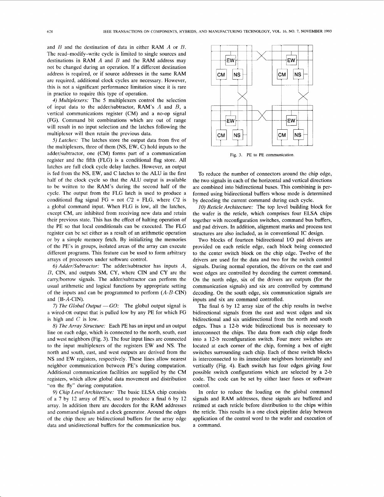
Each PE has an input and an output
line
on
each edge, which is connected to the north, south, east
and west neighbors (Fig.
3).
The four input lines are connected
to the input multiplexers of the registers EW and NS. The
north and south, east, and west outputs are derived from the
NS and EW registers, respectively. These lines allow nearest
neighbor communication between PE’s during computation.
Additional communication facilities are supplied by the CM
registers, which allow global data movement and distribution
“on
the fly” during computation.
9)
Chip Level Architecture:
The basic ELSA chip consists
of
a
7
by 12 array of PE’s, used to produce a final 6 by
12
array.
In
addition there are decoders for the RAM addresses
and command signals and a clock generator. Around the edges
of the chip there are bidirectional buffers for the array edge
data and unidirectional buffers for the communication bus.
7)
The
Global
Output
-GO:
Fig.
3.
PE
to
PE
communication
To reduce the number of connectors around the chip edge,
the two signals in each of the horizontal and vertical directions
are combined into bidirectional buses. This combining is per-
formed using bidirectional buffers whose mode is determined
by decoding the current command during each cycle.
10)
Reticle Architecture:
The top level building block for
the wafer is the reticle, which comprises four ELSA chips
together with reconfiguration switches, command bus buffers,
and pad drivers. In addition, alignment marks and process test
structures are also included, as in conventional IC design.
Two blocks of fourteen bidirectional I10 pad drivers are
provided
on
each reticle edge, each block being connected
to the center switch block
on
the chip edge. Twelve of the
drivers are used for the data and two for the switch control
signals. During normal operation, the drivers on the east and
west edges are controlled by decoding the current command.
On
the north edge, six of the drivers are outputs (for the
communication signals) and six are controlled by command
decoding.
On
the south edge, six communication signals are
inputs and six are command controlled.
The final
6
by 12 array size of the chip results in twelve
bidirectional signals from the east and west edges and six
bidirectional and six unidirectional from the north and south
edges. Thus a 12-b wide bidirectional bus is necessary to
interconnect the chips. The data from each chip edge feeds
into a 12-b reconfiguration switch. Four more switches are
located at each corner of the chip, forming a box of eight
switches surrounding each chip. Each of these switch blocks
is interconnected to its immediate neighbors horizontally and
vertically (Fig.
4).
Each switch has four edges giving four
possible switch configurations which are selected by a 2-b
code. The code can be set by either laser fuses or software
control.
In order to reduce the loading
on
the global command
signals and
RAM
addresses, these signals are buffered and
retimed at each reticle before distribution to the chips within
the reticle. This results in a one clock pipeline delay between
application of the control word to the wafer and execution of
a command.


