
JEDEC Standard No. 79-4C
Page 8
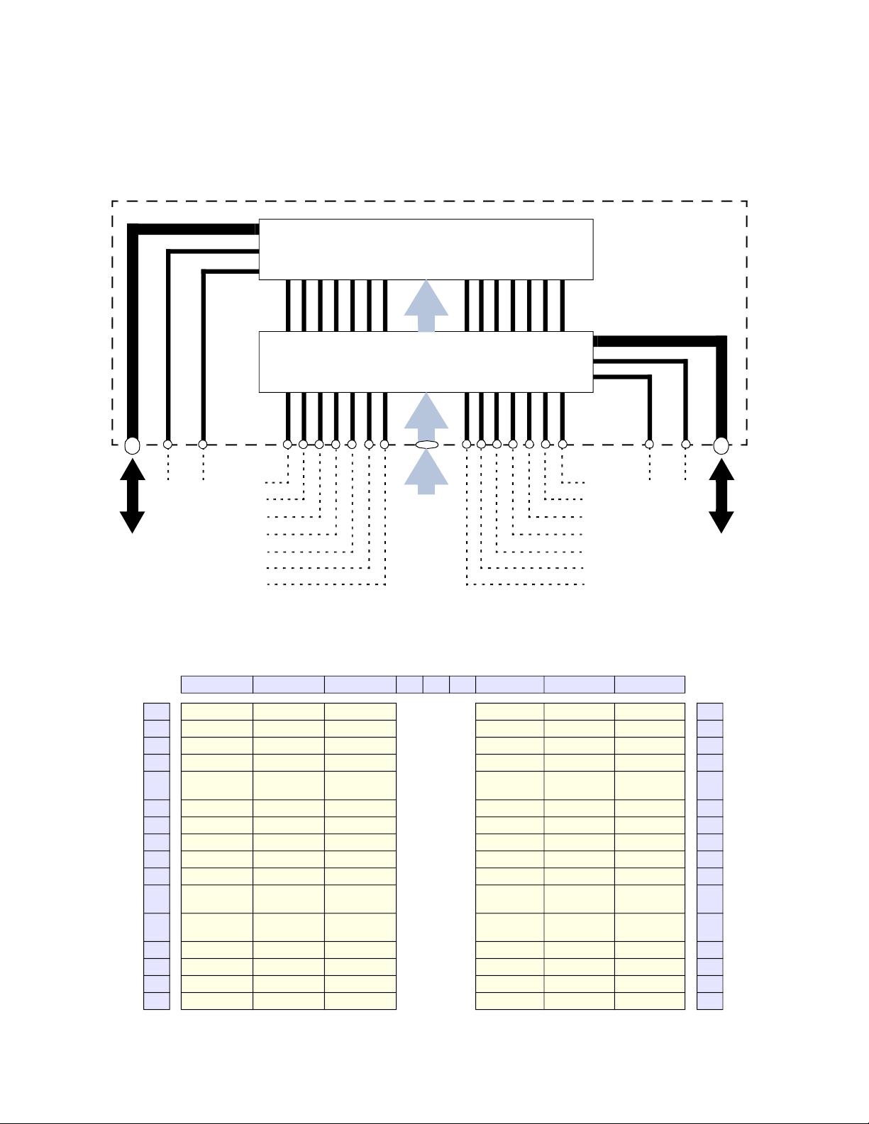
2.9 DDP Single Rank (SR) x16 from two x8
The Single Rank (SR) x16 DDP (Dual Die Package) is comprised of two x8 devices connected in parallel. The intent is to place two
x8 devices in the physical footprint space of a x16. Unless noted otherwise, the functionality, operation, and timings of the SRx16
DDP are to be the same as the mono x8 device.
Figure 4 — Functional Block Diagram of SR x16 DDP
Figure 5 — Ballout of SR x16 DDP using MO-207
1 2 3 4 5 6 7 8 9
A VDDQ VSSQ DQU0 DQSU_c VSSQ VDDQ A
B VPP VSS VDD DQSU_t DQU1 VDD B
C VDDQ DQU4 DQU2 DQU3 DQU5 VSSQ C
D VDD VSSQ DQU6 DQU7 VSSQ VDDQ D
E VSS
DMU_n/
DBIU_n
VSSQ
DML_n
DBIL_n
VSSQ UZQ E
F VSSQ VDDQ DQSL_c DQL1 VDDQ LZQ F
G VDDQ DQL0 DQSL_t VDD VSS VDDQ G
H VSSQ DQL4 DQL2 DQL3 DQL5 VSSQ H
J VDD VDDQ DQL6 DQL7 VDDQ VDD J
K VSS CKE ODT CK_t CK_c VSS K
L VDD
WE_n/
A14
ACT_n CS_n
RAS_n/
A16
VDD L
M VREFCA BG0
A10/
AP
A12/
BC_n
CAS_n/
A15
BG1 M
N VSS BA0 A4 A3 BA1 TEN N
P RESET_n A6 A0 A1 A5 ALERT_n P
R VDD A8 A2 A9 A7 VPP R
T VSS A11 PAR VSS A13 VDD T
Byte 1
(xx Meg x8 x16 banks)
Byte 0
(xx Meg x8 x16 banks)
BG[1:0]
BG[1:0]
BA[1:0]
A[13:0]
UDM_n/
UDBI_n
UZQ
CS_n
RAS_n/A16
CAS_n/A15
WE_n/A14
ACT_n
PAR
VrefCA
LDM_n/
LDBI_n
LZQ
CK_t
CK_c
CKE
ODT
TEN
RESET_n
ALERT_n
UDQ[7:0]
UDQS_t
UDQS_c
LDQ[7:0]
LDQS_t
LDQS_c
--`,``,``,``,,```````,``,-`-``,```,,,`---


剩余265页未读,继续阅读

std86021
- 粉丝: 94
- 资源: 2690
 我的内容管理
收起
我的内容管理
收起
- 我的资源
快来上传第一个资源
 我的收益 登录查看自己的收益
 我的积分
登录查看自己的积分
我的积分
登录查看自己的积分
 我的C币
登录后查看C币余额
我的C币
登录后查看C币余额
 我的收藏
我的收藏  我的下载
我的下载  下载帮助
下载帮助

会员权益专享


最新资源
- 谷歌文件系统下的实用网络编码技术在分布式存储中的应用
- 跨国媒体对南亚农村社会的影响:以斯里兰卡案例的社会学分析
- RFM2g接口驱动操作手册:API与命令行指南
- 基于裸手的大数据自然人机交互关键算法研究
- ABAQUS下无人机机翼有限元分析与局部设计研究
- TCL基础教程:语法、变量与操作详解
- FPGA与数字前端面试题集锦:流程、设计与Verilog应用
- 2022全球互联网技术人才前瞻:元宇宙驱动下的创新与挑战
- 碳排放权交易实战手册(第二版):设计与实施指南
- 2022新经济新职业洞察:科技驱动下的百景变革
- 红外与可见光人脸融合识别技术探究
- NXP88W8977:2.4/5 GHz 双频 Wi-Fi4 + Bluetooth 5.2 合体芯片
- NXP88W8987:集成2.4/5GHz Wi-Fi 5与蓝牙5.2的单芯片解决方案
- TPA3116D2DADR: 单声道数字放大器驱动高达50W功率
- TPA3255-Q1:315W车载A/D类音频放大器,高保真、宽频设计
- 42V 输入 5A 降压稳压器 TPS54540B-Q1 的特点和应用
资源上传下载、课程学习等过程中有任何疑问或建议,欢迎提出宝贵意见哦~我们会及时处理!
点击此处反馈


