Technical Article
.
www.analog.
com
Page 1 of 7 ©2013 Analog Devices, Inc. All rights reserved.
Grasp the Critical Issues for a
Functioning JESD204B
Interface
by Anthony Desimone, Applications Engineer, Analog
Devices, Inc., and Michael Giancioppo, Applications
Engineer, Analog Devices.
JESD204B is a recently approved JEDEC Standard for serial
data interfacing between converters and digital processing
devices. As a third-generation standard, it addresses some of
the limitations of the earlier versions. Among the benefits of
this interface are reductions in required board area for data
interface routing, reductions in setup and hold timing
requirements, and the enablement of smaller packages for
converter and logic devices. New analog/digital converters
from various vendors, such as the AD9250 from Analog
Devices, Inc., use this interface.
There is a trade-off to realizing the benefits of the JESD204B
interface, as it has complexities and subtleties which distinguish
it from existing interface formats and protocols. As with any
standard, it is clear that the interface must function seamlessly
to gain popularity and traction versus more common interfaces,
such as single data rate or double data rate CMOS or LVDS.
Although the JESD204B standard is documented by JEDEC,
some specific information about it is subject to interpretation
or may be spread over multiple references. It is also obvious
that it would be extremely helpful if there were a concise
guide that provided an overview of the standard, how it
works, and how to troubleshoot it if issues arise.
This article explains the interface from an ADC to FPGA for
JESD204B, how to identify when it’s working correctly, and,
perhaps more important, how to troubleshoot it if something
isn’t quite right. The troubleshooting techniques discussed
can use commonly available test and measurement equipment
including oscilloscopes and logic analyzers, along with software
tools such as the ChipScope from Xilinx® or SignalTap from
Altera®. Interface signaling is also explained to allow a single
approach or multiple approaches to visualize the signaling.
JESD204B OVERVIEW
The JESD204B standard provides a method to interface one
or multiple data converters to a digital-signal processing
device (typically, an ADC or DAC to an FPGA) over a higher
speed serial interface compared to the more typical parallel
data transfers. The interface, which runs at up to 12.5 Gbps/
lane, uses a framed serial data link with embedded clock and
alignment characters. The interface eases implementation of
the data interface of high speed converters by reducing the
number of traces between devices, thus reducing trace-
matching requirements, and removing setup- and hold-
timing constraint issues. Since a link needs to be established
prior to data transfer, there are new challenges and techniques
required to identify that the interface is working properly and, if
not, what to do.
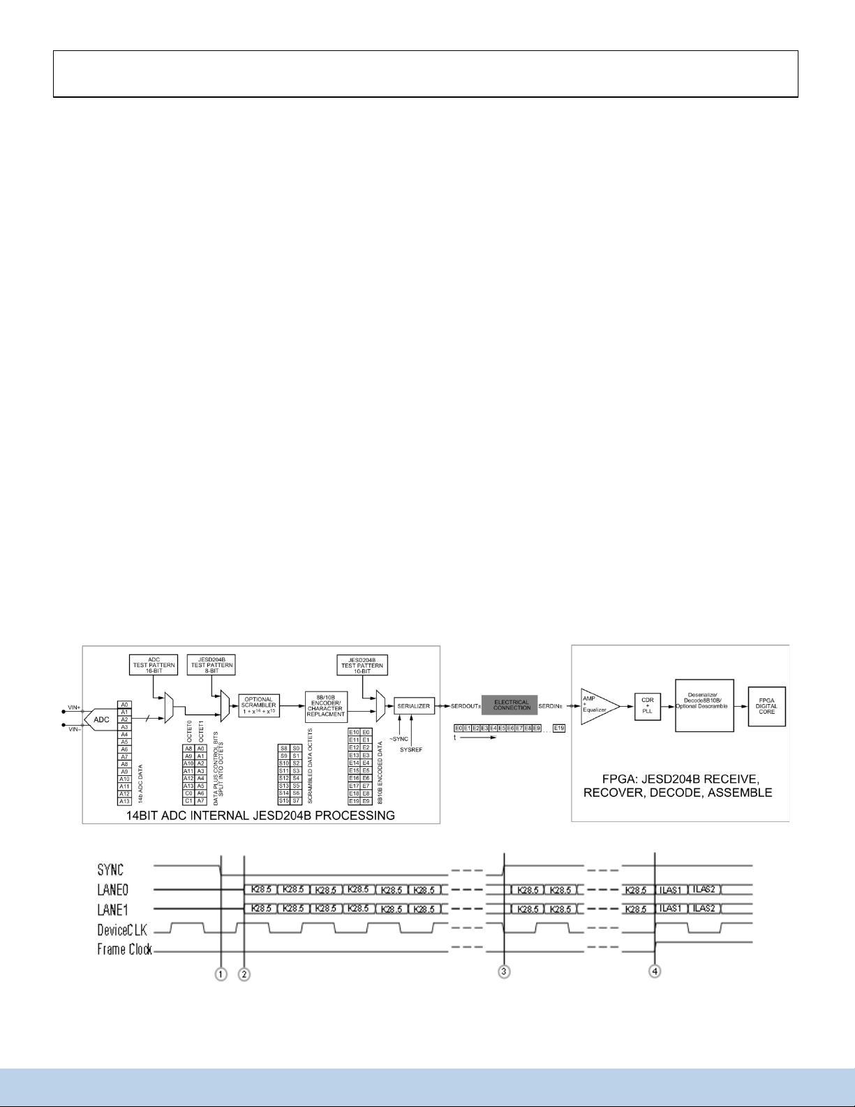
Starting with a brief explanation of how the standard works,
the JESD204B interface uses three phases to establish the
synchronized link: code group synchronization (CGS), initial
lane synchronization (ILAS), and data transmission phase.
Required signals for the link are a shared reference clock
(device clock), at least one differential CML physical data
electrical connection (called a lane), and at least one other
synchronization signal (SYNC~ and possibly SYSREF). The
signals used depend upon the subclass:
• Subclass 0 uses device clock, lanes, and SYNC~
• Subclass 1 uses device clock, lanes, SYNC~, and
SYSREF
• Subclass 2 uses device clock, lanes, and SYNC~
Subclass 0 is adequate in many cases and will be the focus of
this article. Subclass 1 and Subclass 2 provide a method to
establish deterministic latency. This is important in application
when synchronizing multiple devices or system synchroniza-
tion or fixed latency is required (such as when a system needs a
known sampling edge for an event or an event must react to
an input signal within a specified time).
JESD204B Survival Guide
|
14


