■ 8
IEEE CIRCUITS & DEVICES MAGAZINE
■
MAY/JUNE 2005
however, were still too large to make APS commercially viable.
With the advent of deep submicron CMOS and integrated
microlens technologies, APS has made CMOS image sensors a
viable alternative to CCDs. Taking further advantage of tech-
nology scaling, the digital pixel sensor (DPS), first reported in
[6], integrates an ADC at each pixel. The massively parallel
conversion and digital readout provide very high speed read-
out, enabling new applications such as wider dynamic range
(DR) imaging, which is discussed later in this article.
Many of the differences between CCD and CMOS image
sensors arise from differences in their readout architectures.
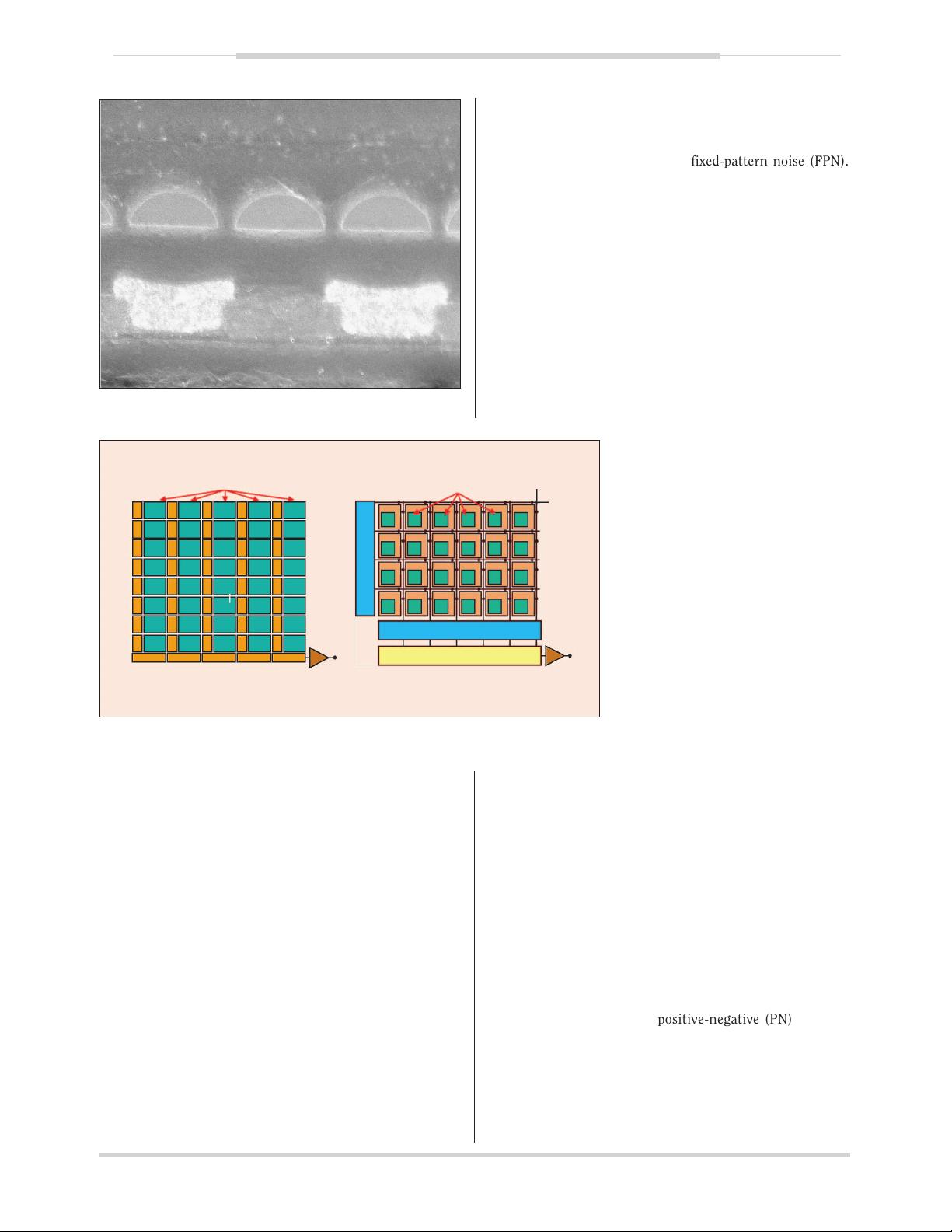
In a CCD [see Figure 4(a)], charge is shifted out of the array
via vertical and horizontal CCDs, converted into voltage via a
simple follower amplifier, and then serially read out. In a
CMOS image sensor, charge voltage signals are read out one
row at a time in a manner similar to a random access memory
using row and column select circuits [see Figure 4(b)]. Each
readout architecture has its advantages and disadvantages.
The main advantage of the CCD readout architecture is that it
requires minimal pixel overhead, making it possible to design
image sensors with very small pixel sizes. Another important
advantage is that charge transfer is passive and therefore does
not introduce temporal noise or pixel to pixel variations due
to device mismatches, known as fixed-pattern noise (FPN).
The readout path in a CMOS image sensor, by comparison,
comprises several active devices that introduce both temporal
noise and FPN. Charge transfer readout, however, is serial
resulting in limited readout speed. It is also high power due to
the need for high-rate, high-voltage clocks to achieve near-
perfect charge transfer efficiency. By comparison, the random
access readout of CMOS image sensors provides the potential
for high-speed readout and window-of-interest operations at
low power consumption. There are several recent examples of
CMOS image sensors operating at hundreds of frames per sec-
ond with megapixel or more resolution [7]–[9]. The high-
speed readout also makes CMOS image sensors ideally suited
for implementing very high-resolution imagers with multi-
megapixel resolutions, especially for
video applications. Recent examples of
such high-resolution CMOS imagers
include the 11-megapixel sensor used
in the Canon EOS-1 camera and the 14-
megapixel sensor used in the Kodak
DCS camera.
Other differences between CCDs and
CMOS image sensors arise from differ-
ences in their fabrication technologies.
CCDs are fabricated in specialized tech-
nologies solely optimized for imaging
and charge transfer. Control over the
fabrication technology also makes it
possible to scale pixel size down with-
out significant degradation in perfor-
mance. The disadvantage of using such
specialized technologies, however, is
the inability to integrate other camera
functions on the same chip with the sensor. CMOS image sen-
sors, on the other hand, are fabricated in mostly standard
technologies and thus can be readily integrated with other
analog and digital processing and control circuits. Such inte-
gration further reduces imaging system power and size and
enables the implementation of new sensor functionalities, as
will be discussed later.
Some of the CCD versus CMOS comparison points made
here should become clearer as we discuss image sensor tech-
nology in more detail.
Photodetection
The most popular types of photodetectors used in image sen-
sors are the reverse-biased positive-negative (PN) junction
photodiode and the P
+
/N/P pinned diode (see Figure 5). The
structure of the pinned diode provides improved photorespon-
sivity (typically with enhanced sensitivity at shorter wave-
lengths) relative to the standard PN junction [10]. Moreover,
the pinned diode exhibits lower thermal noise due to the pas-
sivation of defect and surface states at the Si/SiO
2
interface, as
3. A cross-section SEM photograph of an image sensor showing the
microlens and CFA deposited on top of the photodetectors.


