Left Channel Right Channel
n-1 n-2 n-3 3 2 1 0 n-1n-2n-3 3 2 1
n-1 n-2 n-3
LD(n)
Ch_Offset_1 = 0
RD(n)
Ch_Offset_1 = 0
LD(n+1)
WORD
CLOCK
BIT
CLOCK
DATA
LD(n) = nth Sample of Left-Channel Data
RD(n) = nth Sample of Left-Channel Data
3
Left Channel Right Channel
n-1 n-2 n-3 3 2
1
0 n-1 n-2 n-3 3 2 1 0
n-1 n-2 n-3
LD(n)
RD(n)
LD(n+1)
WORD
CLOCK
BIT
CLOCK
DATA
LD(n) = nth Sample of Left-Channel Data
RD(n) = nth Sample of Left-Channel Data
Ch_Offset_1 = 1
Ch_Offset_1 = 1
16
TLV320ADC3100
ZHCSHY2 –MARCH 2018
www.ti.com.cn
版权 © 2018, Texas Instruments Incorporated
Feature Description (接接下下页页)
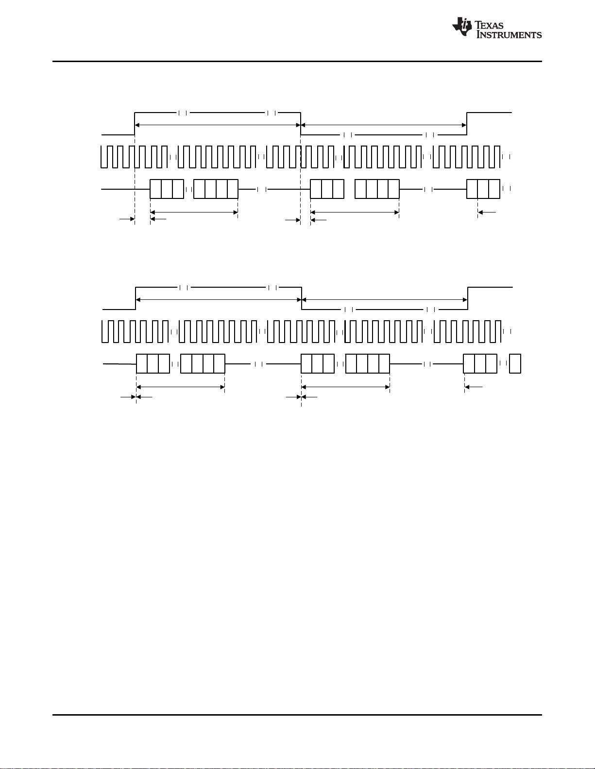
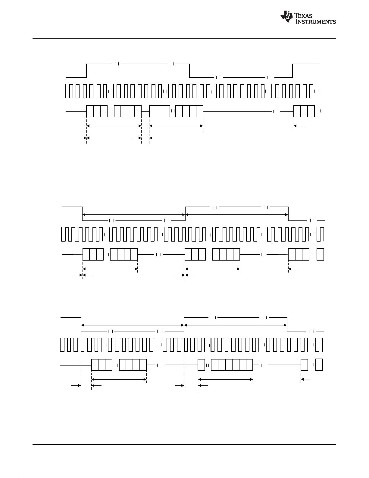
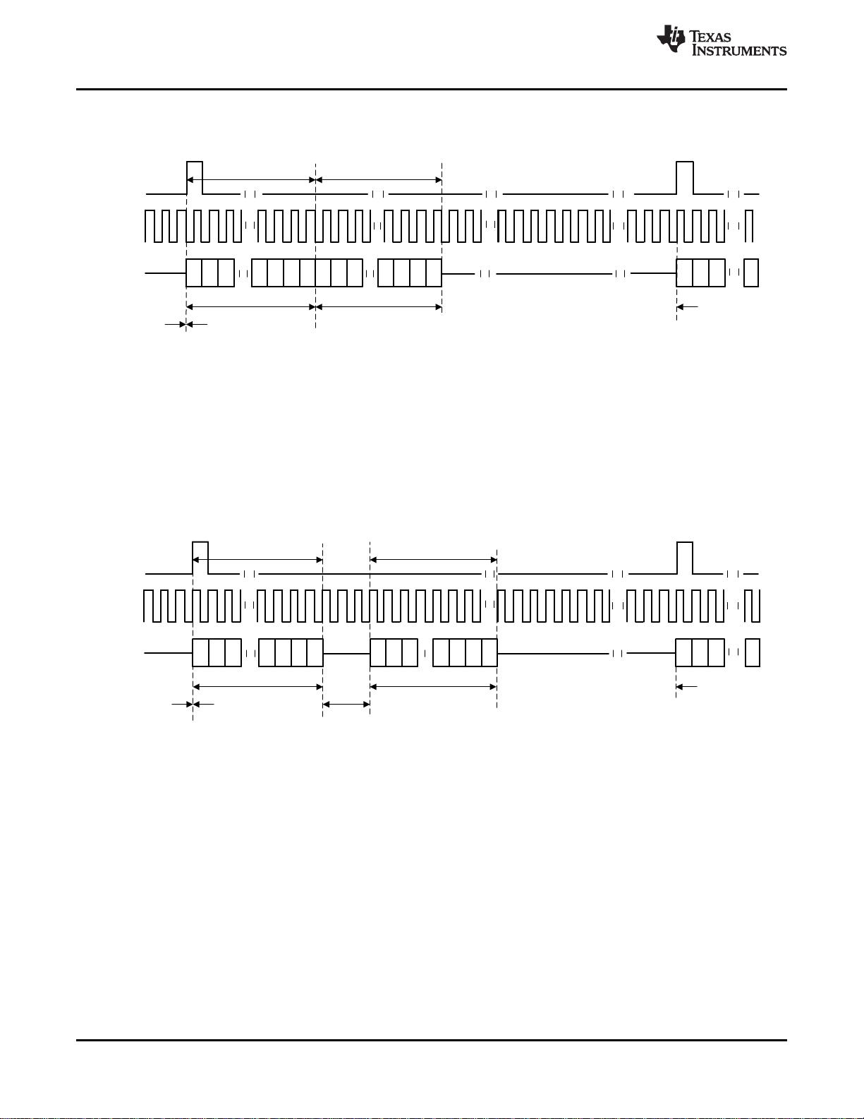
图 14 shows the left-justified mode with Ch_Offset_1 = 1.
图图 14. Left-Justified Mode With Ch_Offset_1 = 1
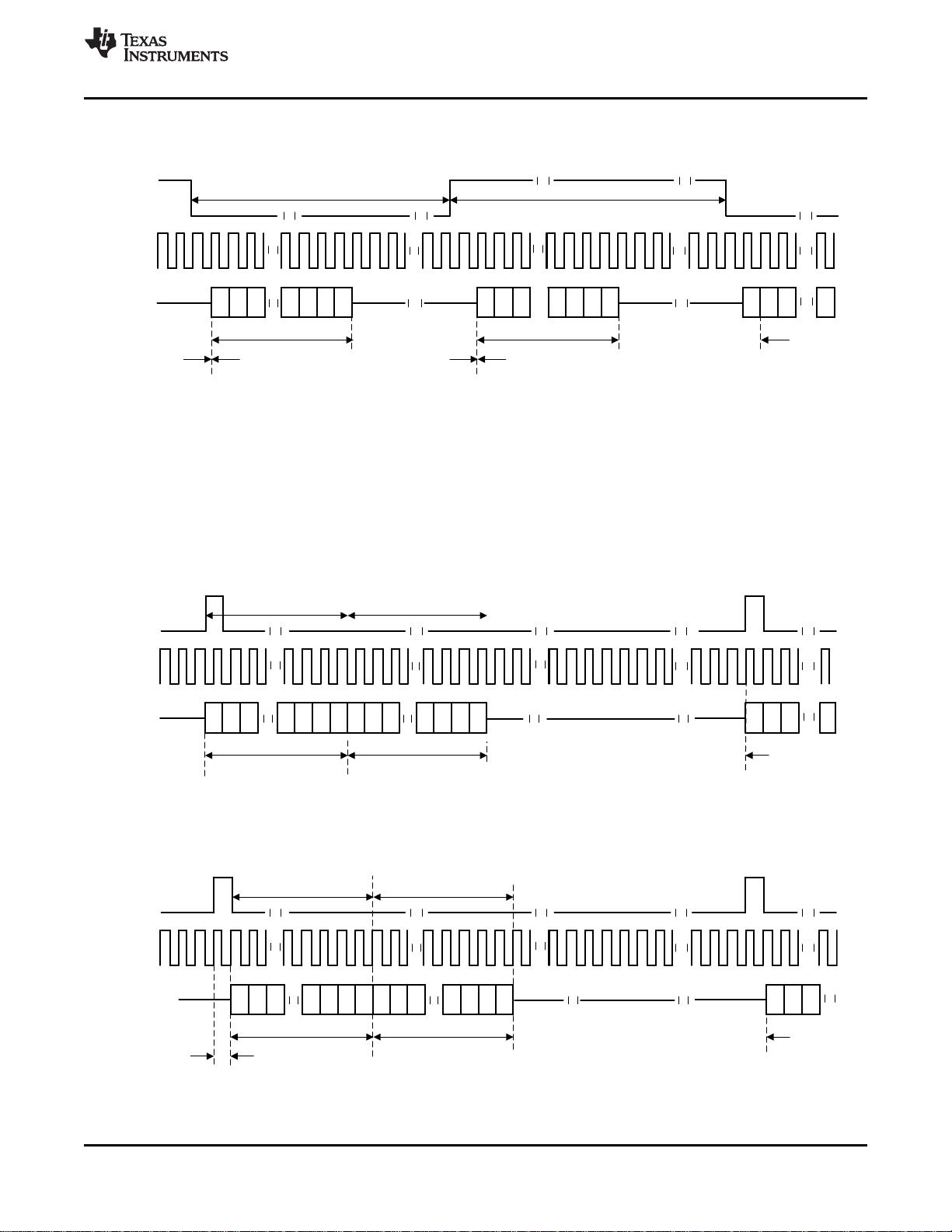
图 15 shows the left-justified mode with Ch_Offset_1 = 0 and bit clock inverted.
图图 15. Left-Justified Mode With Ch_Offset_1 = 0, Bit Clock Inverted
For left-justified mode, the number of bit clocks per frame must be greater than twice the programmed word
length of the data. Also, the programmed offset value must be less than the number of bit clocks per frame by at
least the programmed word length of the data.
When the time-slot-based channel assignment is disabled (page 0, register 38, bit 0 = 0), the left and right
channels have the same offset Ch_Offset_1 (page 0, register 28), and each edge of the word clock starts data
transfer for one of the two channels, depending on whether or not channel swapping is enabled. Data bits are
valid on the rising edges of the bit clock. With the time-slot-based channel assignment enabled (page 0, register
38, bit 0 = 1), the left and right channels have independent offsets (Ch_Offset_1 and Ch_Offset_2). The rising
edge of the word clock starts data transfer for the first channel after a delay of its programmed offset
(Ch_Offset_1) for this channel. Data transfer for the second channel starts after a delay of its programmed offset
(Ch_Offset_2) from the LSB of the first-channel data. The falling edge of the word clock is not used.
With no channel swapping, the MSB of the left channel is valid on the (Ch_Offset_1 + 1)th rising edge of the bit
clock following the rising edge of the word clock. Consequently, the MSB of the right channel is valid on the
(Ch_Offset_1 + 1)th rising edge of the bit clock following the falling edge of the word clock. The timing diagram of
图 14 illustrates the operation in this case, with an offset of 1. Because channel swapping is not enabled, the left-
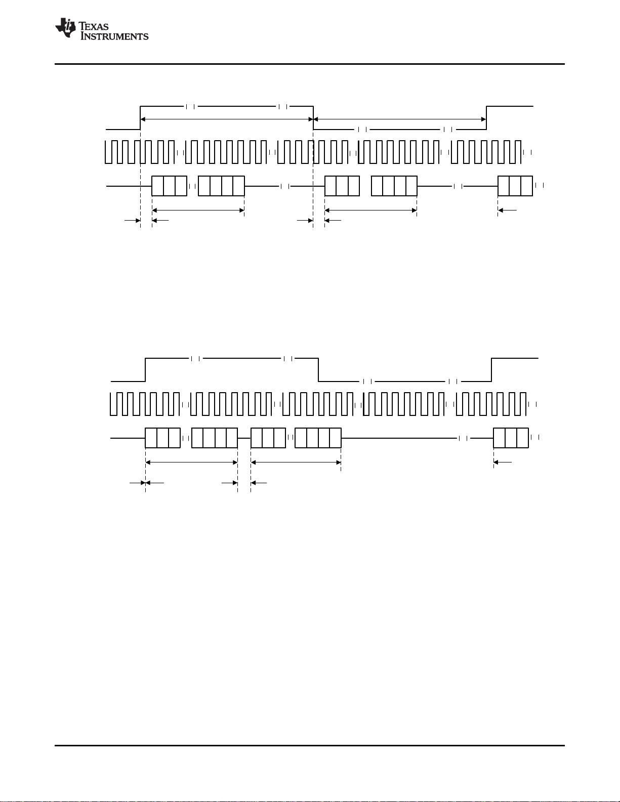
channel data are before the right-channel data. With channel swapping enabled, the MSB of the right channel is
valid on the (Ch_Offset_1 + 1)th rising edge of the bit clock following the rising edge of the word clock. Thus, the
MSB of the left channel is valid on the (Ch_Offset_1 + 1)th rising edge of the bit clock following the falling edge
of the word clock. The timing diagram of 图 16 depicts the operation in this case, with an offset of 1. As shown in
the diagram, the right-channel data of a frame are before the left-channel data of that frame because of channel
swapping. Otherwise, the behavior is similar to the case where channel swapping is disabled. The MSB of the
right-channel data is valid on the second rising edge of the bit clock after the rising edge of the word clock, as a
result of an offset of 1. Similarly, the MSB of the left-channel data is valid on the second rising edge of the bit
clock after the falling edge of the word clock.


