1704 IEEE JOURNAL OF SOLID-STATE CIRCUITS, VOL. 55, NO. 6, JUNE 2020
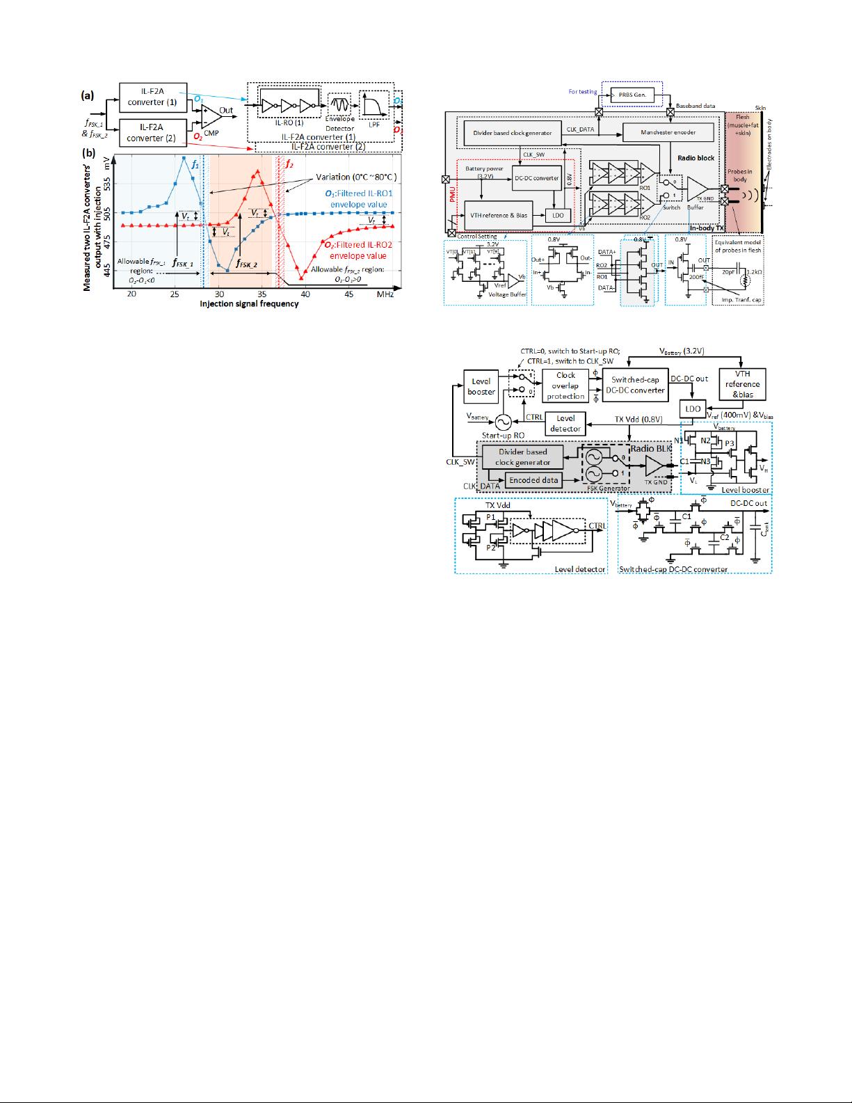
To improve the PMU efficiency, a 1/3-switched-cap dc–dc
converter is first used to convert the 3.2-V battery voltage into
about 1.1 V before passing it to LDO. The LDO then regulates
the dc–dc output to 0.8 V, outputting a current of 10.5 µA
while maintaining the output supply ripple to within 1%. The
dc–dc converter is switched by a clock signal derived from
one RO within the TX FSK generator. The clock frequency is
obtained by passing the RO through a 1/64 divider. 500 kHz is
chosen for the resulting clock signal (CLK_SW) as well as the
baseband clock (CLK_DATA) to achieve the desired 500-kb/s
data rate. By reusing RO within the FSK generator for clock
generation, it reduces the overall PMU power consumption
after startup.
Although the PMU architecture is straightforward, there
exists a startup issue that deserves some discussion. This issue
arises due to reusing RO for clock generation to achieve power
saving. This is because RO is powered by PMU, which might
not be functioning if the switching clock is not available.
Hence, an auto clock switching scheme is adopted here to
eliminate this startup issue. During the startup phase, a simple
inverter-based RO directly powered by the micro-battery will
be used to drive the PMU with an oscillation frequency
of 200–300 kHz. Lower frequency is chosen here to reduce
the startup power consumed by the PMU. This clock will
be used by the dc–dc converter until the LDO output is
sufficient to power up the ROs within the FSK generator.
In our PMU design, once the LDO output attains 0.5 V,
a level detector will automatically switch the clock signal
from micro-battery-powered RO to the RO within the FSK
generator. To reduce area and power of PMU, two PMOS
pseudoresistors in series are employed to generate a reference
voltage, which is half of TX Vdd. This reference voltage
will drive a resistive load inverter (P1 and P2). By sizing
P1 and P2 appropriately, the inverter will switch when TX
Vdd reaches 0.5 V. The level detector output, CTRL, will then
toggle the PMU clock signal from micro-battery-powered RO
to CLK_SW automatically. Once the auto clock switching is
done, the startup RO will be powered down to save power.
In the PMU, a ULP VTH reference [35] will provide a
supply insensitive 400-mV reference to the LDO. It will also
be used to generate bias needed for all blocks within the TX.
A charge pump is employed to drive the switched-cap network.
It converts the periodic 500-kHz CLK_SW signal at low volt-
age (0–0.8 V) into full micro-battery voltage level (0 ∼ 3.2 V)
while consuming less than 85 nW. Non-overlapping clock
generator is also used to avoid simultaneous turning on of
the switches.
C. On-Body RX
As mentioned earlier, the lack of accurate reference clock
for the implanted TX results in significant frequency fluctua-
tion. To overcome this issue, IL-F2A-based frequency varia-
tion resilient demodulator discussed earlier is shown in Fig. 9.
In the RX, the received signal from the two on-body
electrodes is first amplified by a three-stage bandpass front-end
amplifier (FEA) with 50-dB gain. An on-chip balun cou-
pled with inverters converts the single-ended signal into
pseudo-differential full swing signal to minimize the common
Fig. 9. Schematic of the on-body RX.
mode noise and enlarge the dynamic range. As the on-body
electrodes within the galvanic-couple I2O-BCC band exhibits
relatively high impedance, a simple self-biased inverter archi-
tecture is adopted as the FEA. The same current-starved
pseudo-differential inverter architecture is adopted in both
the injection and delay cells. The injection strength can be
tuned by digitally adjusting the tail transistor sizing ratio. The
desired injection strength of 0.1 is determined based on the
simulation and measurement. This value will generate two
wide regions (light blue and light red in Fig. 6) for proper
demodulation of the two TX FSK frequencies despite their
potential large variations. The two three-stage current-starved
pseudo-differential ROs are free running at different frequen-
cies. Their center frequencies should be adjusted roughly to
fall within the I2O-BCC band. A simple differential rectifier
coupled with RC filter is employed as ED. Additional second-
order LPF is used to extract the average value of the two
IL-F2A outputs. The ED exhibits conversion gain around 0 dB,
a bandwidth of 1.5 MHz, and output noise less than 400 µV
PP
.
To achieve a minimum SNR of 20 dB, the ED output voltage
needs to be at least 4 mV
PP
. By taking into TX output voltage,
the channel loss, and the ED output voltage requirement,
the desired FEA gain can be found. The LPF-dB gain is
with bandwidth of 1.5 MHz. The LPF output corresponding
to the two IL-F2As is then sent to a differential regenerative
current feedback Schmitt trigger as shown in Fig. 6(b). The
Schmitt trigger is designed to have a hysteresis of 300 mV. The
amplitude difference between the two IL-F2A outputs can be
adjusted by tuning the RC value of the ED, the common mode
of the LPF, and the input offset of the Schmitt trigger. The
demodulated data will then pass through a Manchester decoder
to extract both the baseband data and clock information.
VI. M
EASUREMENT RESULTS
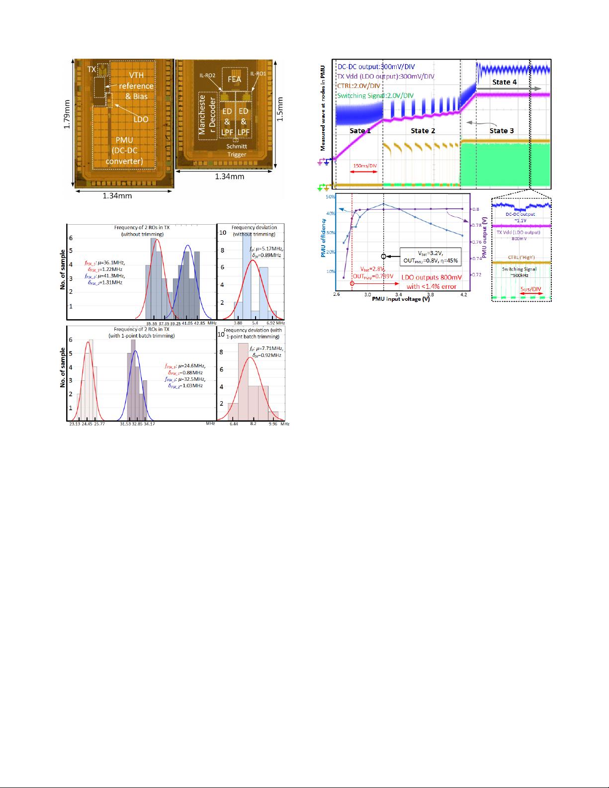
Fabricated in Global Foundries 130-nm CMOS technology,
the in-body TX and on-body RX die photos are shown
in Fig.10.
A. Implanted TX
As the TX with on-chip PMU will be implanted in human
body, we expect the major contribution to the FSK frequency
variation would be from the process variation. It should
be noted that to reduce the cost, batch trimming should
Authorized licensed use limited to: ShanghaiTech University. Downloaded on May 30,2020 at 12:20:29 UTC from IEEE Xplore. Restrictions apply.


