COL 10(1), 013103(2012) CHINESE OPTICS LETTERS January 10, 2012
Thinning and polishing of cross-section of depth-graded
WSi
2
/Si multilayer for linear zone plate application
Qiushi Huang (黄黄黄秋秋秋实实实)
1, 2
, Jingtao Zhu (朱朱朱京京京涛涛涛)
1, 2∗
, Haochuan Li (李李李浩浩浩川川川)
1, 2
, Zhengxiang Shen (沈沈沈正正正祥祥祥)
1, 2
,
Xiaoqiang Wang (王王王晓晓晓强强强)
1, 2
, Zhanshan Wang (王王王占占占山山山)
1, 2
, and Yongjian Tang (唐唐唐永永永建建建)
3
1
Institute of Precision Optical Engineering, Physics Department, Tongji University, Shanghai 200092, China
2
Shanghai Key Lab oratory of Special Artif icial Microstructure Materials and Technology, Tongji University,
Shanghai 200092, China
3
Research Center of Laser Fusion, China Academy of Engineering Physics, Mianyang 621900, China
∗
Corresp onding author: jtzhu@tong ji.edu.cn
Received April 11, 2011; accepted June 14, 2011; posted online August 24, 2011
A linear zone plate named multilayer laue lens (MLL) is fabricated using a depth-graded multilayer struc-
ture. The lens shows considerable potential in focusing an X-ray beam into a nanometer scale with high
efficiency. In this letter, a depth-graded multilayer consisting of 324 alternating WSi
2
and Si layers with
a total thickness of 7.9 µm is deposited based on the thickness sequence according to the demands of
the zone plate law. Subsequently, the multilayer sample is sliced and thinned to an ideal depth along
the cross-section direction using raw abrasives and diamond lapping. Finally, the cross-section is polished
by a chemical mechanical polishing (CMP) technique to remove the damages and improve the surface
smoothness. The final depth of the MLL is approximately 7 µm with an achieved aspect ratio greater
than 400. Results of scanning electron microscopy (SEM) and atomic force microscopy (AFM) indicate
that interfaces are sharp, and the multilayer structure remains undamaged after the thinning and polishing
processes. The surface roughness achieved is 0.33 nm.
OCIS co des: 310.3840, 340.7460, 310.1860.
doi: 10.3788/COL201210.013103.
High-brilliance synchrotron X-ray sources enhance the
feasibility of nanobeam focusing, which is helpful to X-
ray microscopy analysis under higher resolution. Several
components have been developed to focus X-rays into
a nanobeam, such as Kirkpatrick-Baez mirrors
[1]
, com-
pound refractive lens
[2]
, Fresnel zone plate lens
[3]
, and
graded multilayer mirrors
[4]
. Fresnel zone plates have
been demonstrated as powerful focusing lenses in X-ray
microscopy applications. However, for hard X-rays, the
aspect ratio of a zone plate (ratio of the depth of a zone
plate to its outermost zone width) becomes exceedingly
large that could not be achieved using traditional litho-
graphic techniques. A novel linear zone plate, named
multilayer laue lens (MLL), is developed by depositing
the depth-graded multilayer reversely on flat substrates
and subsequently slicing and polishing the lens to achieve
a larger aspect ratio. As a result, MLL has shown capa-
bility to provide a significantly higher focusing efficiency
and resolution especially in hard X-ray regions
[5,6]
. Fur-
thermore, the outermost layers (i.e., the thinnest layers)
of MLL, which determine the resolution, are firstly de-
posited on a substrate to control the thicknesses and
quality of the critical layers better. A MLL structure
with an outermost layer thickness of 5 nm has focused
the 19.5-keV X-ray into a line focus of 16 nm, with an
efficiency of 31%
[7]
.
In this letter, a MLL is designed and a thickness-graded
multilayer with 324 layers is successfully dep osited using
WSi
2
and Si alternately. The detailed slicing, thinning,
and polishing processes of the multilayer sample are re-
ported to form a nearly perfect linear zone plate with a
high aspect ratio.
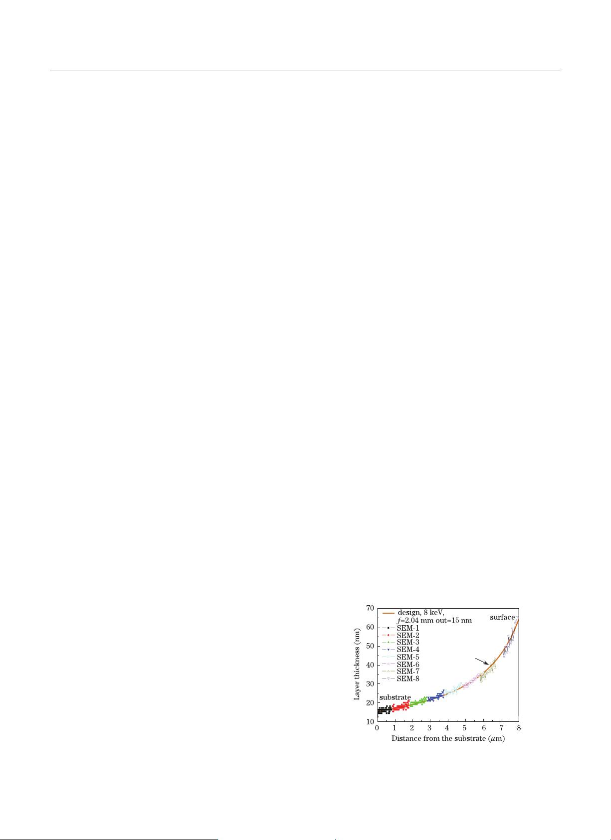
The MLL was designed at energy E=8 keV, with a
focal length of 2.04 mm. According to the zone plate
law, the depth-graded multilayer should consist of 324
alternating WSi
2
and Si layers with a total thickness
of 7.9 µm. The outermost layer thickness of the zone
plate is 15 nm. In the present study, the layer thickness
increases from 15 to 65 nm as shown in Fig. 1.
The material combination of WSi
2
/Si was chosen to
fabricate the MLL because of its stable stress property
[8]
.
To ensure better control of the position and quality of the
outermost layers, which determine the focusing property,
the multilayer was deposited reversely on a super pol-
ished Si(100) substrate using direct current magnetron
sputtering technology
[9,10]
. After deposition, the cross-
section of the multilayer was observed by scanning elec-
tron microscopy (SEM), as shown in Fig. 2. Figure
2(a) is an image of the entire cross-section, and Fig. 2(b)
Fig. 1. Designed and deposited multilayer structure of MLL.
The total number of layers is 324 with a total thickness of 7.9
µm.
1671-7694/2012/013103(4) 013103-1
c
° 2012 Chinese Optics Letters


