18 www.xilinx.com 7 Series FPGAs Memory Interface Solutions
UG586 January 18, 2012
Chapter 1: DDR3 and DDR2 SDRAM Memory Interface Solution
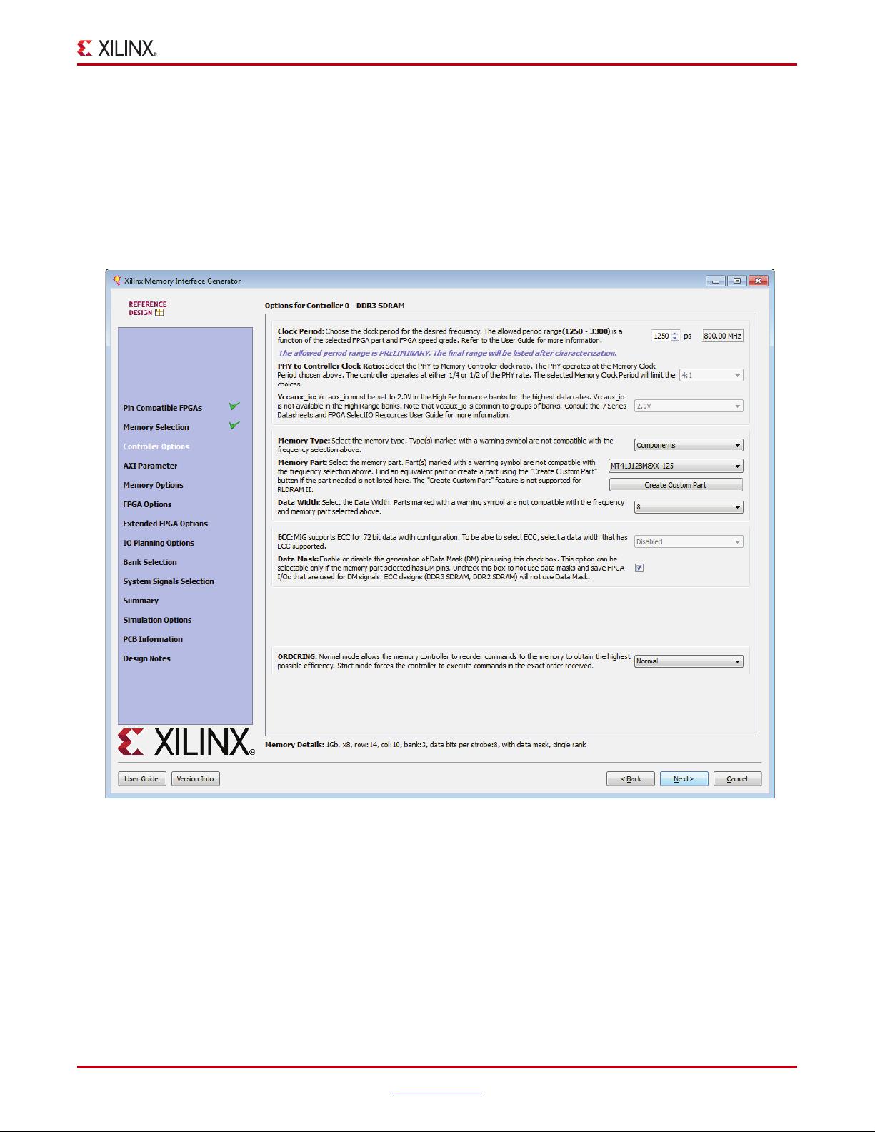
If the design has multiple controllers, the controller options page is repeated for each of the
controllers. This page is partitioned into a maximum of nine sections. The number of
partitions depends on the type of memory selected. The controller options page also
contains these pull-down menus to modify different features of the design:
• Frequency: This feature indicates the operating frequency for all the controllers. The
frequency block is limited by factors such as the selected FPGA and device speed
grade. In the EDK flow, an extra check box (selected by default) allows the user to
specify that the frequency information should be calculated automatically from EDK.
• Input Clock Period: The desired input clock period is selected from the list. These
values are determined by the memory clock period chosen and the allowable limits of
the parameters. See Design Guidelines, page 126 for more information on the PLL
parameter limits.
• PHY to Controller Clock Ratio: This feature determines the ratio of the physical layer
(memory) clock frequency to the controller and user interface clock frequency. The 2:1
ratio lowers the maximum memory interface frequency due to fabric timing
limitations. The user interface data bus width of the 2:1 ratio is 4 times the width of
the physical memory interface width, while the bus width of the 4:1 ratio is 8 times the
physical memory interface width. The 2:1 ratio has lower latency. The 4:1 ratio is
necessary for the highest data rates.
• Vccaux_io: Vccaux_io is set based on the period/frequency setting. 2.0V is required at
the highest frequency settings in the High Performance column. The MIG tool
automatically selects 2.0V when required. Either 1.8 or 2.0V can be used at lower
frequencies. Groups of banks share the Vccaux_io supply. See the 7 Series FPGAs
SelectIO Resources User Guide [Ref 1] and the 7 Series FPGAs Packaging and Pinout
Specification [Ref 2] for more information.
• Memory Type: This feature selects the type of memory parts used in the design.
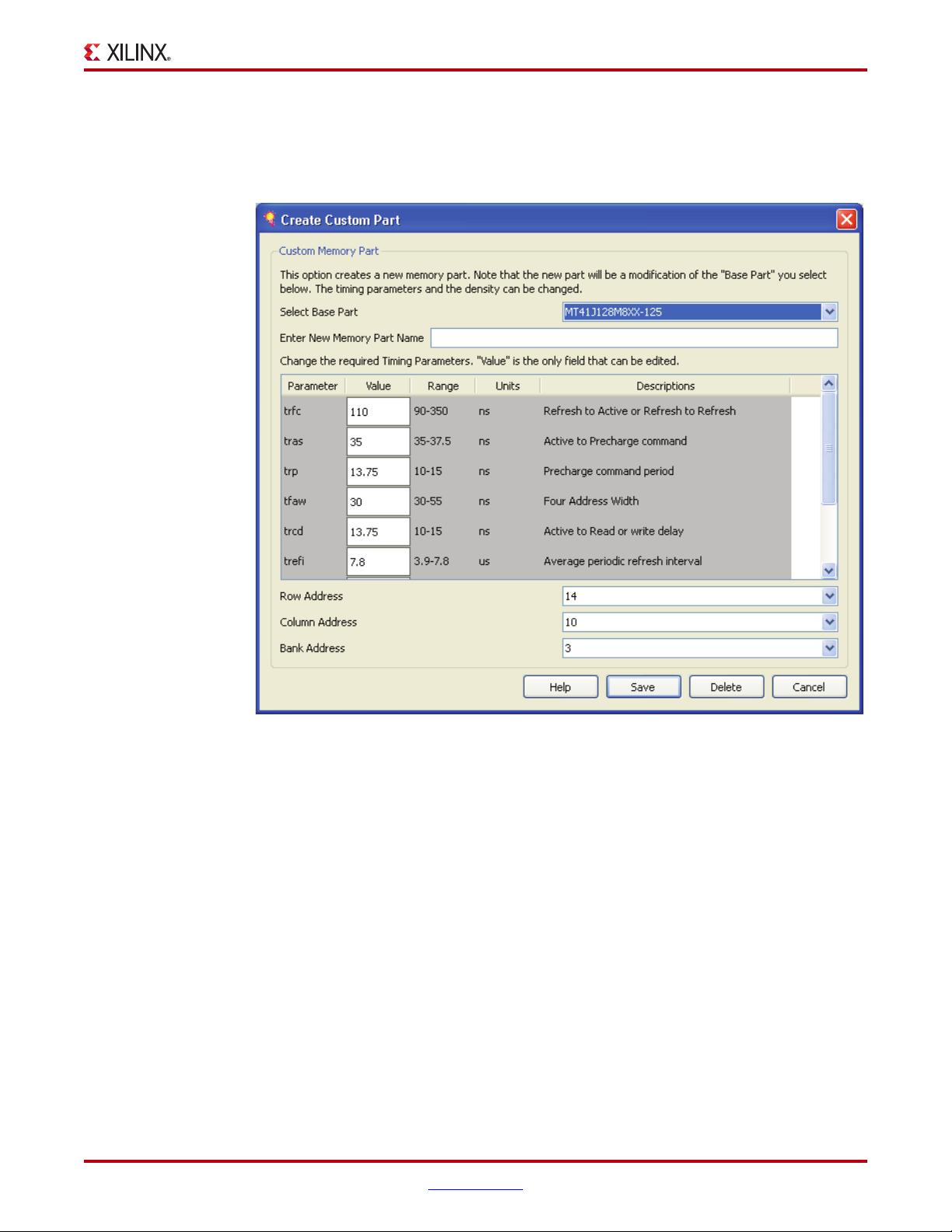
• Memory Part: This option selects a memory part for the design. Selections can be
made from the list or a new part can be created.
• Data Width: The data width value can be selected here based on the memory type
selected earlier. The list shows all supported data widths for the selected part. One of
the data widths can be selected. These values are generally multiples of the individual
device data widths. In some cases, the width might not be an exact multiple. For
example, 16 bits is the default data width for x16 components, but 8 bits is also a valid
value.
• Data Mask: This option allocates data mask pins when selected. This option should
be deselected to deallocate data mask pins and increase pin efficiency. This option is
disabled for memory parts that do not support data mask.
• Ordering: This feature allows the memory controller to reorder commands to
improve the memory bus efficiency.
• Memory Details: The bottom of the Controller Options page (Figure 1-11, page 17)
displays the details for the selected memory configuration (Figure 1-12).
1. Select the appropriate frequency. Either use the spin box or enter a valid value using
the keyboard. Values entered are restricted based on the minimum and maximum
frequencies supported.
X-Ref Target - Figure 1-12
Figure 1-12: Memory Details
UG586_c1_20_091410


