16
DS110DF1610
SNLS472A –JANUARY 2014–REVISED JUNE 2017
www.ti.com
Product Folder Links: DS110DF1610
Submit Documentation Feedback Copyright © 2014–2017, Texas Instruments Incorporated
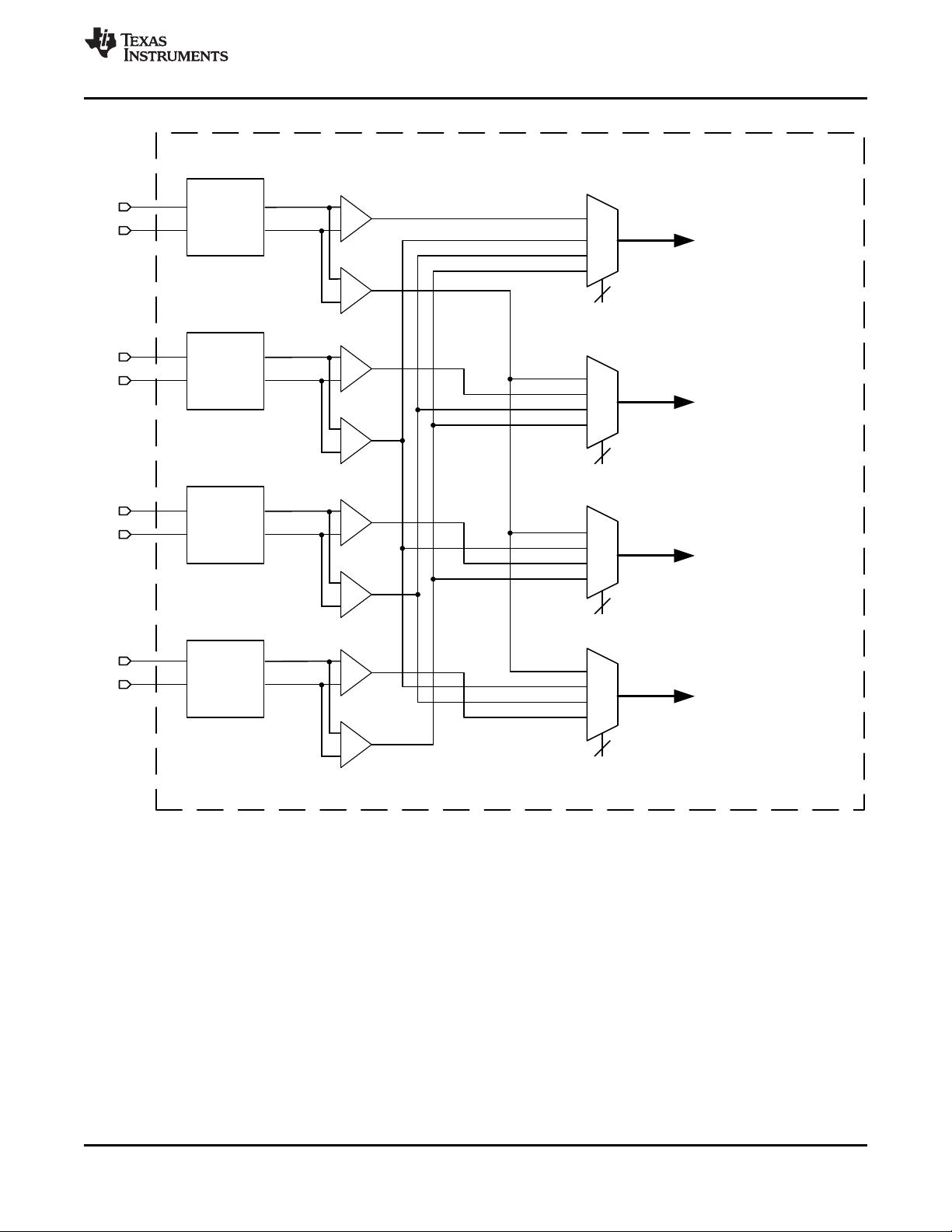
• 1:4 – any channel input to all 4 channels output
When the cross point switch is configured to replicate/broadcast data a master must be assigned during the
cross point configuration. The master channel will have control over the CTLE adaption. All of the slave channels
will be able to adapt their own DFE, but will not have control to adapt the CTLE. In this type of configuration there
must be 1 channel assigned as a master. All other channels in the broadcast network must be assigned as
slaves. There cannot be more than one master channel in a broadcast network.
In a typical data replication/broadcast application users must configure the following for each channel:
1. Control bus mux setting (ch reg 0x9B)
2. Data path mux setting (ch reg 0x96)
3. Enabling/Disabling the local or multi-drive buffers for each channel (ch reg 0x96)
4. Master/Slave assignment (ch reg 0x96)
5. Cross point enable bit (ch reg 0x96)
6. Perform a CDR reset and reset release (ch reg 0x0A)
6.3.1.4 DFE With VGA
A 5-tap DFE with a VGA can be enabled within the data path of each channel to assist with reducing the effects
of cross talk, reflections, or post cursor inter-symbol interference (ISI). The DFE must be manually enabled,
regardless of the selected adapt mode. Once the DFE has been enabled it can be configured to adapt only
during lock acquisition or to adapt continuously. The DFE can also be manually configured to specified tap
polarities and tap weights. However, when the DFE is configured manually the DFE auto-adaption should be
disabled.
The DFE taps are all feedback taps with 1UI spacing. Each tap has a specified boost weight range and polarity
bit.
DFE PARAMETER VALUE (mV)
Tap 1 Weight Range 0 – 224
Tap 2-5 Weight Range 0 – 112
Tap Weight Step Size 7
A VGA is located at the input to the DFE block. The VGA has 2-bit control to allow for 4 levels of boost. The VGA
can be used to assist in the recovery of extremely small signals. Note that the VGA is integrated within the DFE,
so in order to use the VGA the DFE must be enabled.
6.3.1.5 Clock and Data Recovery
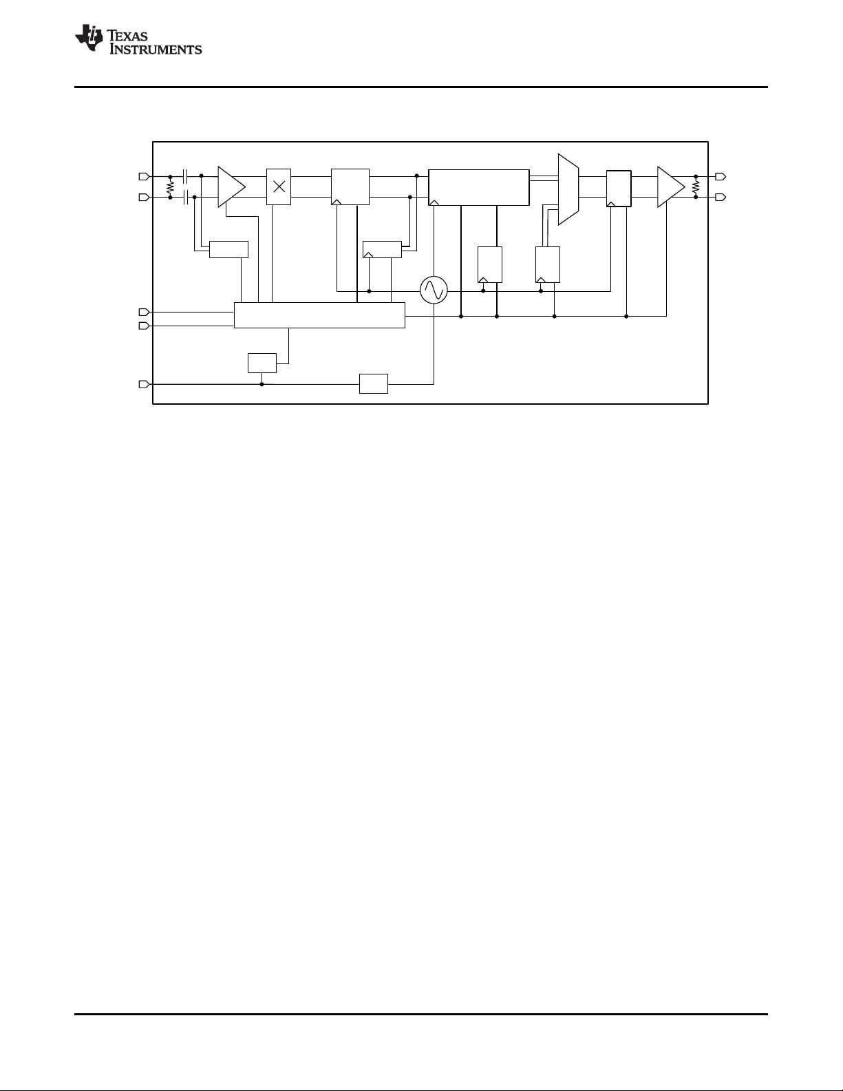
The CDR block consists of a Phase Locked Loop (PLL), reference clock based PPM counter, Input and Output
Data Multiplexers (mux) and circuits to monitor single bit transitions and detect false locking. The CDR sampling
position is fixed at the 0.5UI location for each bit.
By default, the equalized data is fed into the CDR for clock and data recovery. This data is then output to FIR
filter and differential driver. Users can configure the CDR data to route the recovered clock and data to the PRBS
checker. Users also have the option of configuring the output of the CDR to send raw non-retimed data, or data
from the pattern generator.
The CDR requires the following in order to be properly configured:
• Input reference clock with proper reference clock divider setting to run the PPM counter.
• Expected data rates must be programmed into the CDR either through the rate/sub-rate table or entered
manually with the corrected divider settings.
6.3.1.6 Reference Clock
The reference clock is not part of the CDR’s PLL. The reference clock is connected only to the PPM counter for
each CDR. The PPM counter constrains the allowable lock ranges of the CDR according to the programmed
values in the rate/sub-rate table or the manually entered data rates.
