ANALOG INPUTS AND MULTIPLEXER
AVSS 0.7V<(AINNorAINP)<AVDD 1.25V- -
(1)
NOISE PERFORMANCE
IDLE TONES
OPERATING MODE
S
1
S
2
S
3
S
4
S
5
S
6
AINP1
AINP2
AINN2
AINN1
AVSS
AVDD
S
7
(+)
( )-
ToPGA
AVDD+AVSS
2
400W
400W
ADS1282
SBAS418A – SEPTEMBER 2007 – REVISED DECEMBER 2007
The RESET input resets the register settings and
also restarts the conversion process. The PWDN
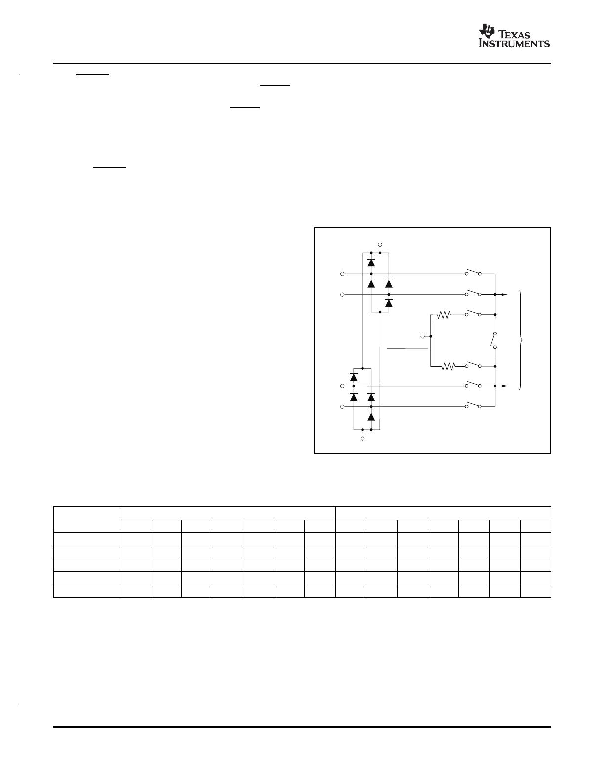
A diagram of the input multiplexer is shown in
input sets the device into a micro-power state. Note
Figure 2 . The specified input operating range of the
that register settings are not retained in PWDN mode.
inputs are shown in Equation 1 :
Use the STANDBY command in its place if it is
desired to retain register settings (the quiescent
current in the Standby mode is slightly higher).
ESD diodes protect the multiplexer inputs. If either
input is taken below AVSS – 0.3V or above AVSS +
Noise-immune Schmitt-trigger and clock-qualified
0.3V, the ESD protection diodes may turn on. If these
inputs ( RESET and SYNC) provide increased
conditions are possible, external Schottky clamp
reliability in high-noise environments. The serial
diodes and/or series resistors may be required to limit
interface is used to read conversion data, in addition
the input current to safe values (see the Absolute
to reading and writing to the configuration registers.
Maximum Ratings table).
The ADS1282 offers outstanding noise performance
(SNR). SNR depends on the data rate and the PGA
setting. As the bandwidth is decreased by decreasing
the data rate, the SNR improves correspondingly.
Table 1 summarizes the typical noise performance
with inputs shorted.
The ADS1281 modulator incorporates an internal
dither signal that randomizes the idle tone energy.
Low-level idle tones may still be present, typically
– 137dB below full-scale. The low-level idle tones can
be shifted out of the passband with the application of
an external 20mV offset.
For applications where minimal power consumption is
important, the low-power mode can be selected
(register bit MODE = 0). In low-power mode, the
power is reduced from 27mW to 17mW and SNR
Figure 2. Analog Inputs and Multiplexer
degrades by 3dB.
Table 1. Noise Performance (Typical
(1)
)
PGA (High-Resolution Mode) PGA (Low-Power Mode)
DATA RATE
(SPS) 1 2 4 8 16 32 64 1 2 4 8 16 32 64
250 130 130 129 128 125 119 114 127 127 126 125 122 116 111
500 127 127 126 125 122 116 111 124 124 123 122 119 113 108
1000 124 124 123 122 119 113 108 121 121 120 119 116 110 105
2000 121 121 120 119 116 111 106 118 118 117 116 113 108 103
4000 118 118 117 116 113 108 103 115 115 114 113 110 105 100
(1) V
IN
= 20mV
DC
.
8 Submit Documentation Feedback Copyright © 2007, Texas Instruments Incorporated
Product Folder Link(s): ADS1282


