汽车级9位1.3GSPS ADC09xJ1300-Q1:高性能激光雷达应用
需积分: 13 37 浏览量
更新于2024-06-28
4
收藏 6.99MB PDF 举报
"TI-ADC09QJ1300-Q1.pdf 是一款由TI公司推出的汽车级高性能模拟数字转换器(ADC),专为满足激光雷达(LiDAR)系统的严苛要求而设计。这款9位、1.3GSPS的ADC具备多种通道配置,包括四通道、双通道和单通道,且符合AEC-Q100第一温度等级的车规标准,工作范围在-40°C至+125°C之间。"
TI的ADC09QJ1300-Q1拥有诸多显著特性,首先,其内核是9位分辨率的ADC,最高采样率可达1.3GSPS,采用非交错式架构,能有效减少内部抖动,从而降低高次谐波的影响。在性能规格方面,当输入信号为-1dBFS时,它在100MHz时的信噪比(SNR)为53.5dBFS,等效无杂散动态范围(SFDR)为64dBc,而本底噪声低至-143dBFS。此外,ADC的满量程输入电压为800mVPP-DIFF,全功率输入带宽高达6GHz,这使得它能够处理高速信号。
该器件支持JESD204C串行数据接口,可以配置为2至8个(四通道/双通道)或1至4个(单通道)串行器/解串器通道,最大波特率可达17.16Gbps,支持64B/66B和8B/10B编码模式,并具备子类1的确定性延迟功能,同时保持与JESD204B接收器的兼容性。ADC09QJ1300-Q1还提供了内部采样时钟生成,内部集成的PLL和VCO工作在7.2-8.2GHz的范围内,有助于简化系统设计。
为了便于系统同步,ADC09QJ1300-Q1提供了一个SYSREF窗口,并有四个时钟输出,可以为FPGA、相邻ADC或串行器/解串器收发器提供参考时钟。此外,还配备了脉冲系统的时间戳输入和输出功能,这对于时间敏感的应用至关重要。
在功耗方面,根据通道数量的不同,功耗分别为:四通道每通道450mW,双通道每通道625mW,单通道940mW。该ADC需要1.1V和1.9V的电源电压。封装选项为FCBGA(144),尺寸为10.0mm×10.0mm。
此ADC系列适用于高精度、高速的汽车应用,特别是激光雷达系统,其6GHz的全功率输入带宽使得它在FMCW LiDAR和脉冲式LiDAR系统中表现出色,同时支持直接射频采样,最高可达4GHz,展现了其在高频信号处理领域的卓越性能。
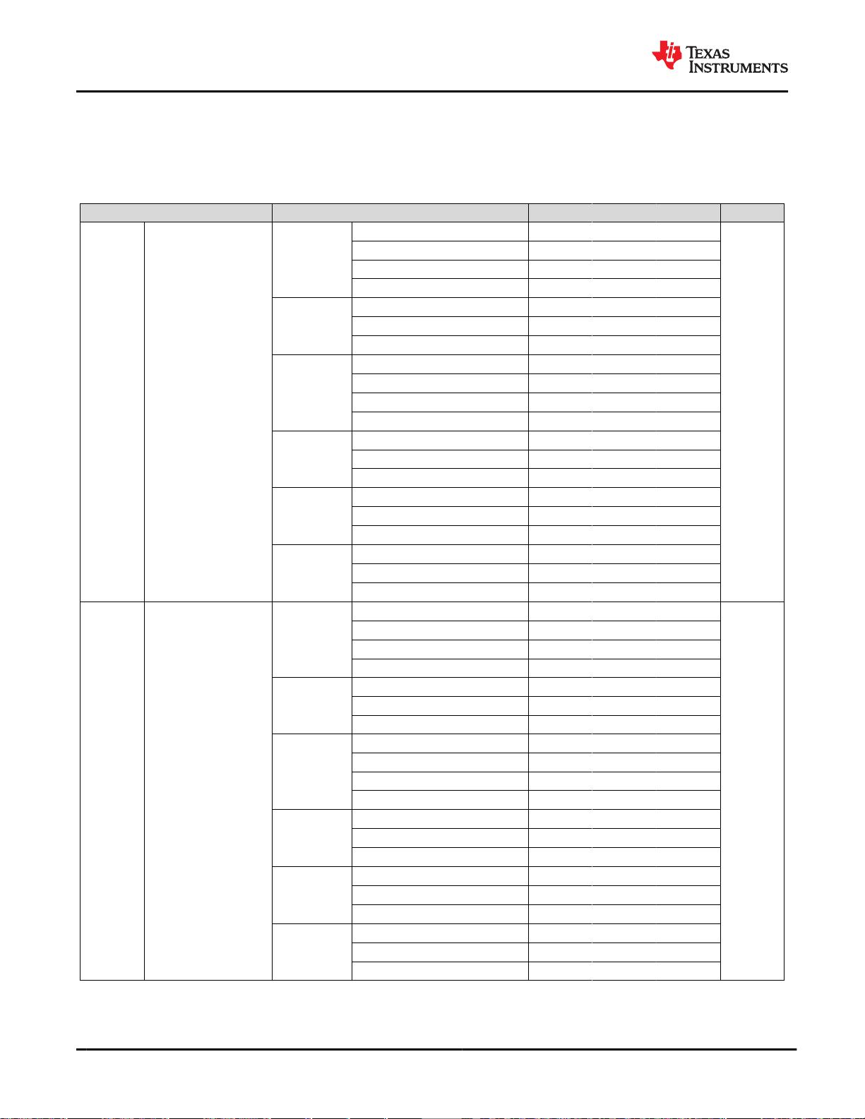
7.6 Electrical Characteristics: Power Consumption
typical values at T
A
= 25°C, VA19 = 1.9 V, VPLL19 = 1.9 V, VREFO = 1.9 V, VTRIG = 1.1V, VA11 = 1.1 V, VD11 = 1.1 V,
default full-scale voltage (V
FS
= 0.8 V
PP
), f
IN
= 97 MHz, A
IN
= –1 dBFS, f
CLK
= 1.3 GHz, filtered 1-V
PP
sine-wave clock
applied to CLK±, PLL disabled, JMODE = 0, High Performance Mode and foreground calibration (unless otherwise noted);
minimum and maximum values are at nominal supply voltages and over the operating free-air temperature range provided in
the Recommended Operating Conditions table
PARAMETER TEST CONDITIONS MIN TYP MAX UNIT
I
VA19
1.9-V analog supply current
Power mode 1a: Quad channel, JMODE 0
(9-bit, 8 lanes, 8B/10B encoding), FG
calibration, PLL_EN = 0, f
S
= 1.3 GSPS,
High Performance Mode
667 mA
I
VPLL19
PLL analog supply current 0 mA
I
VREFO
PLLREFO± analog supply current 0 mA
I
VTRIG
TRIGOUT± analog supply current 0 mA
I
VA11
1.1-V analog supply current 576 mA
I
VD11
1.1-V digital supply current 600 mA
P
DIS
Power dissipation 2.56 W
I
VA19
1.9-V analog supply current
Power mode 1b: Duad channel, JMODE 0
(9-bit, 8 lanes, 8B/10B encoding), FG
calibration, PLL_EN = 0, fS = 1.3 GSPS,
High Performance Mode
385 mA
I
VPLL19
PLL analog supply current 0 mA
I
VREFO
PLLREFO± analog supply current 0 mA
I
VTRIG
TRIGOUT± analog supply current 0 mA
I
VA11
1.1-V analog supply current 452 mA
I
VD11
1.1-V digital supply current 379 mA
P
DIS
Power dissipation 1.64 W
I
VA19
1.9-V analog supply current
Power mode 1c: Single channel, JMODE
0 (9-bit, 8 lanes, 8B/10B encoding), FG
calibration, PLL_EN = 0, fS = 1.3 GSPS,
High Performance Mode
257 mA
I
VPLL19
PLL analog supply current 0 mA
I
VREFO
PLLREFO± analog supply current 0 mA
I
VTRIG
TRIGOUT± analog supply current 0 mA
I
VA11
1.1-V analog supply current 419 mA
I
VD11
1.1-V digital supply current 236 mA
P
DIS
Power dissipation 1.2 W
I
VA19
1.9-V analog supply current
Power mode 2a: Quad channel, JMODE 8
(9-bit, 4 lanes, 64B/66B encoding), LPBG
calibration, PLL_EN = 0, f
S
= 1.0 GSPS,
Low Power Mode
565 mA
I
VPLL19
PLL analog supply current 0 mA
I
VREFO
PLLREFO± analog supply current 0 mA
I
VTRIG
TRIGOUT± analog supply current 0 mA
I
VA11
1.1-V analog supply current 400 mA
I
VD11
1.1-V digital supply current 387 mA
P
DIS
Power dissipation 1.95
(1)
W
I
VA19
1.9-V analog supply current
Power mode 2b: Dual channel, JMODE 8
(9-bit, 4 lanes, 64B/66B encoding), LPBG
calibration, PLL_EN = 0, f
S
= 1.0 GSPS,
Low Power Mode
347 mA
I
VPLL19
PLL analog supply current 0 mA
I
VREFO
PLLREFO± analog supply current 0 mA
I
VTRIG
TRIGOUT± analog supply current 0 mA
I
VA11
1.1-V analog supply current 344 mA
I
VD11
1.1-V digital supply current 239 mA
P
DIS
Power dissipation 1.3
(1)
W
I
VA19
1.9-V analog supply current
Power mode 2c: Single channel, JMODE
8 (9-bit, 4 lanes, 64B/66B encoding),
LPBG calibration, PLL_EN = 0, f
S
= 1.0
GSPS, Low Power Mode
240 mA
I
VPLL19
PLL analog supply current 0 mA
I
VREFO
PLLREFO± analog supply current 0 mA
I
VTRIG
TRIGOUT± analog supply current 0 mA
I
VA11
1.1-V analog supply current 322 mA
I
VD11
1.1-V digital supply current 179 mA
P
DIS
Power dissipation 1.01
(1)
W
ADC09QJ1300-Q1, ADC09DJ1300-Q1, ADC09SJ1300-Q1
ZHCSKU9A – FEBRUARY 2020 – REVISED JUNE 2021
www.ti.com.cn
16 Submit Document Feedback
Copyright © 2021 Texas Instruments Incorporated
Product Folder Links: ADC09QJ1300-Q1 ADC09DJ1300-Q1 ADC09SJ1300-Q1

剩余158页未读,继续阅读
点击了解资源详情
点击了解资源详情
点击了解资源详情
2022-11-27 上传
2022-11-27 上传
2022-11-27 上传
2022-11-27 上传
2022-11-27 上传
2022-11-27 上传

不觉明了
- 粉丝: 6313
- 资源: 5764
 我的内容管理
展开
我的内容管理
展开


最新资源
- 毕业设计&课设--分享一个适合初学者的图书管理系统(毕业设计)无框架原生.zip
- marvel_api
- Chrome-Memory-Manager:此扩展仅在 chrome 的开发者频道上有效。 Chrome合金
- Broad-Learning-System:BLS代码
- 毕业设计&课设--东北大学本科毕业设计模板.zip
- mcmc_clib:C程序简化ODE模型参数的歧管MALA采样
- yii2-meta-activerecord:一个简单的Yii2扩展,扩展了ActiveRecord功能,以允许在补充表中使用WordPress样式的元字段
- job-recover-client:JobRecover的客户端文件(前端)
- TestDrive-Titanium:使用这个空白的 Titanium 应用程序试驾 Kinvey
- final-form-focus::chequered_flag:最终表单“装饰器”,它将在尝试提交表单时尝试将焦点应用于第一个字段,但会出现错误
- keras-recommendation:使用Keras实施推荐系统
- Excel模板年度工程类中初级打分汇总表.zip
- GoIT-Course:这是我在GoIT课程中的第二门课程
- 毕业设计&课设--高校毕业设计管理系统(毕业设计).zip
- PyTorchZeroToAll:DL-SEMINAR第1周任务
- Geo_Aggs-Map
