TLC2543C, TLC2543I, TLC2543M
12-BIT ANALOG-TO-DIGITAL CONVERTERS
WITH SERIAL CONTROL AND 11 ANALOG INPUTS
SLAS079F – DECEMBER 1993 – REVISED NOVEMBER 2001
6
POST OFFICE BOX 655303 • DALLAS, TEXAS 75265
operating characteristics over recommended operating free-air temperature range,
V
CC
= V
ref+
= 4.5 V to 5.5 V, f
(I/O
CLOCK)
= 4.1 MHz
PARAMETER TEST CONDITIONS MIN TYP
†
MAX UNIT
E
L
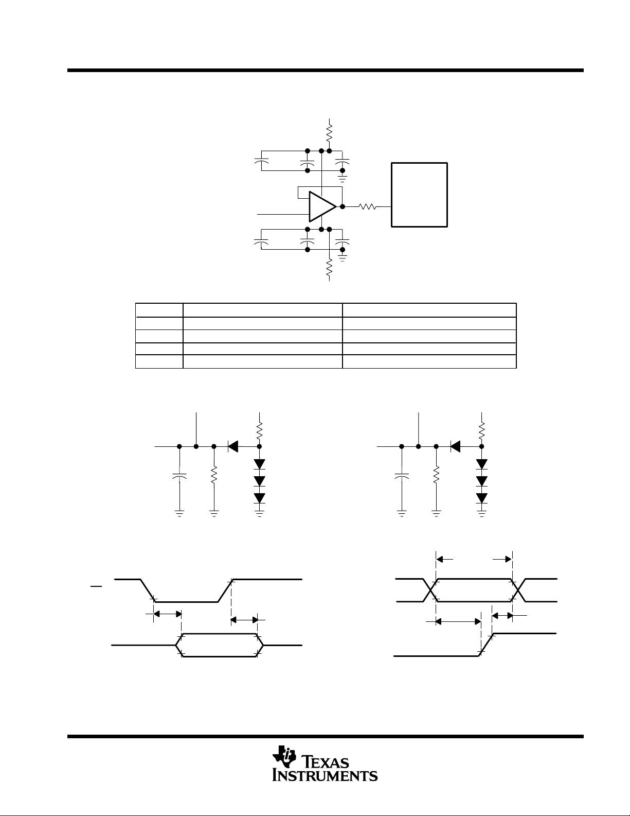
Linearity error (see Note 5) See Figure 2 ±1 LSB
E
D
Differential linearity error See Figure 2 ±1 LSB
E
O
Offset error (see Note 6)
See Note 2 and
Figure 2
±1.5 LSB
E
G
Gain error (see Note 6)
See Note 2 and
Figure 2
±1 LSB
E
T
Total unadjusted error (see Note 7) ±1.75 LSB
DATA INPUT = 1011 2048
Self-test output code (see Table 3 and Note 8)
DATA INPUT = 1100
0
DATA INPUT = 1101 4095
t
(conv)
Conversion time See Figures 9–14 8 10 µs
t
c
Total cycle time (access, sample, and conversion)
See Figures 9–14
and Note 9
10 + total
I/O CLOCK
periods +
t
d(I/O-EOC)
µs
t
acq
Channel acquisition time (sample)
See Figures 9–14
and Note 9
4 12
I/O
CLOCK
periods
t
v
Valid time, DATA OUT remains valid after I/O CLOCK↓ See Figure 6 10 ns
t
d(I/O-DATA)
Delay time, I/O CLOCK↓ to DATA OUT valid See Figure 6 150 ns
t
d(I/O-EOC)
Delay time, last I/O CLOCK↓ to EOC↓ See Figure 7 1.5 2.2 µs
t
d(EOC-DATA)
Delay time, EOC↑ to DATA OUT (MSB/LSB) See Figure 8 100 ns
t
PZH
, t
PZL
Enable time, CS↓ to DATA OUT (MSB/LSB driven) See Figure 3 0.7 1.3 µs
t
PHZ
, t
PLZ
Disable time, CS↑ to DATA OUT (high impedance) See Figure 3 70 150 ns
t
r(EOC)
Rise time, EOC See Figure 8 15 50 ns
t
f(EOC)
Fall time, EOC See Figure 7 15 50 ns
t
r(bus)
Rise time, data bus See Figure 6 15 50 ns
t
f(bus)
Fall time, data bus See Figure 6 15 50 ns
t
d(I/O-CS)
Delay time, last I/O CLOCK↓ to CS↓ to abort conversion
(see Note 10)
5 µs
†
All typical values are at T
A
= 25°C.
NOTES: 2. Analog input voltages greater than that applied to REF+ convert as all ones (111111111111), while input voltages less than that
applied to REF– convert as all zeros (000000000000).
5. Linearity error is the maximum deviation from the best straight line through the A/D transfer characteristics.
6. Gain error is the difference between the actual midstep value and the nominal midstep value in the transfer diagram at the specified
gain point after the offset error has been adjusted to zero. Offset error is the difference between the actual midstep value and the
nominal midstep value at the offset point.
7. Total unadjusted error comprises linearity, zero-scale, and full-scale errors.
8. Both the input address and the output codes are expressed in positive logic.
9. I/O CLOCK period = 1/(I/O CLOCK frequency) (see Figure 7).
10. Any transitions of CS
are recognized as valid only when the level is maintained for a setup time. CS must be taken low at ≤ 5 µs
of the tenth I/O CLOCK falling edge to ensure a conversion is aborted. Between 5 µs and 10 µs, the result is uncertain as to whether
the conversion is aborted or the conversion results are valid.


