Data Sheet AD9959
Rev. C | Page 9 of 44
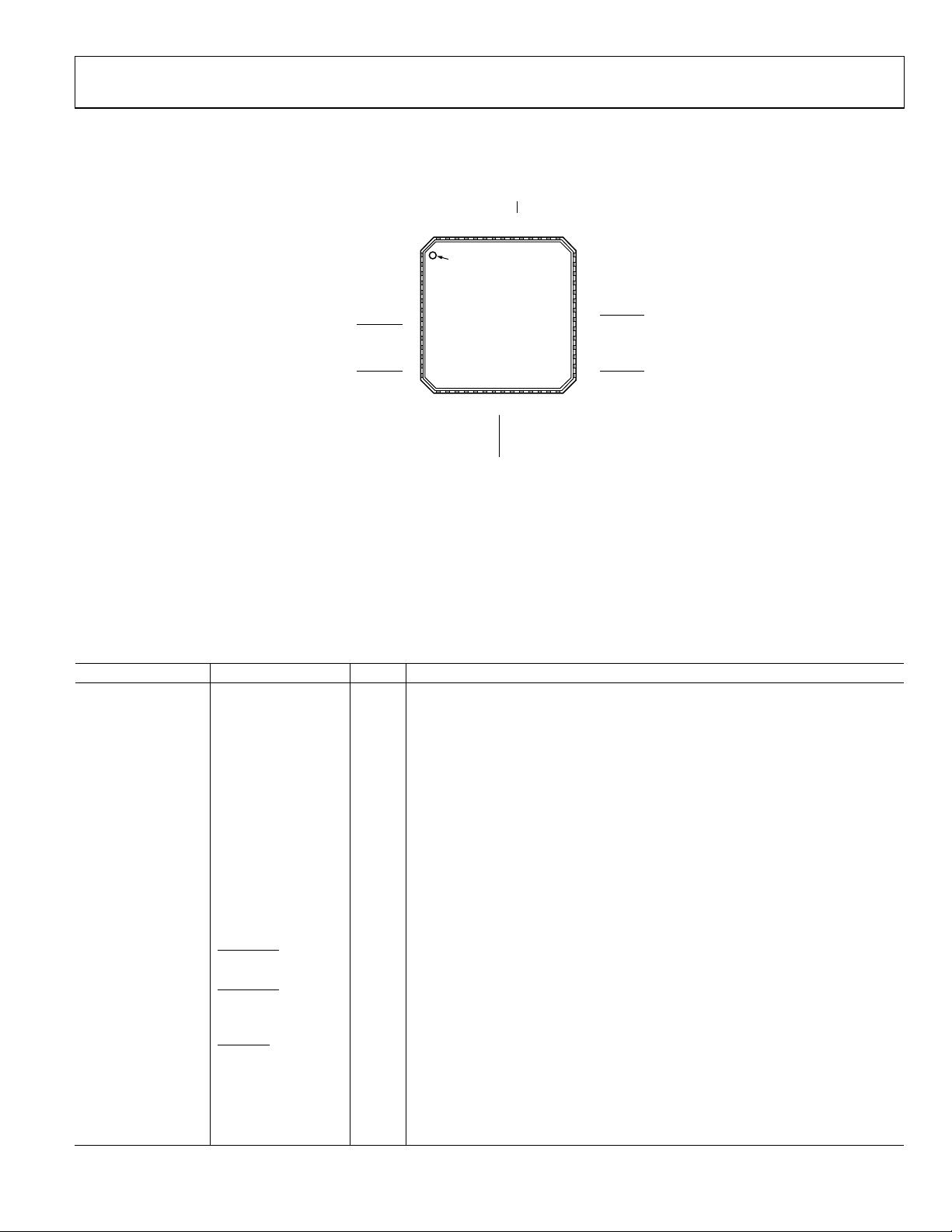
PIN CONFIGURATION AND FUNCTION DESCRIPTIONS
PIN 1
INDICATOR
NC = NO CONNECT
1
SYNC_IN
2
SYNC_OUT
3
MASTER_RESET
4
PWR_DWN_CTL
5
AVDD
6
AGND
7
AVDD
8
CH2_IOUT
9
CH2_IOUT
10
AGND
11
AVDD
12
AGND
13
CH3_IOUT
14
CH3_IOUT
35
CH1_IOUT
36
CH1_IOUT
37
AVDD
38
AGND
39
AVDD
40
P0
41
P1
42
P2
34
AGND
33
AVDD
32
AGND
31
AVDD
30
CH0_IOUT
29
CH0_IOUT
15
AVDD
16
AGND
17
DAC_RSET
19
AVDD
21
AVDD
20
AGND
22
REF_CLK
23
REF_CLK
24
CLK_MODE_SEL
25
AGND
26
AVDD
27
LOOP_FILTER
28
AGND
18
AGND
45
DVDD
46
I/O_UPDATE
47
CS
48
SCLK
49
DVDD_I/O
50
SDIO_0
51
SDIO_1
52
SDIO_2
53
SDIO_3
54
SYNC_CLK
44
DGND
43
P3
TOP VIEW
(Not to Scale)
AD9959
55
DVDD
56
DGND
05246-003
NOTES
1. THE EXPOSED EPAD ON BOTTOM SIDE OF PACKAGE IS
AN ELECTRICAL CONNECTION AND MUST BE
SOLDERED TO GROUND.
2. PIN 49 IS DVDD_I/O AND IS TIED TO 3.3V.
Figure 3. Pin Configuration
Table 3. Pin Function Descriptions
Pin No. Mnemonic I/O
1
Description
1 SYNC_IN I Used to Synchronize Multiple AD9959 Devices. Connects to the SYNC_OUT pin of
the master AD9959 device.
2 SYNC_OUT O Used to Synchronize Multiple AD9959 Devices. Connects to the SYNC_IN pin of the
slave AD9959 devices.
3 MASTER_RESET I Active High Reset Pin. Asserting the MASTER_RESET pin forces the AD9959 internal
registers to their default state, as described in the Register Maps and Bit Descriptions
section.
4 PWR_DWN_CTL I External Power-Down Control.
5, 7, 11, 15, 19, 21,
26, 31, 33, 37, 39
AVDD I Analog Power Supply Pins (1.8 V).
6, 10, 12, 16, 18, 20,
25, 28, 32, 34, 38
AGND I Analog Ground Pins.
45, 55 DVDD I Digital Power Supply Pins (1.8 V).
44, 56 DGND I Digital Power Ground Pins.
8 CH2_IOUT O True DAC Output. Terminates into AVDD.
9
CH2_IOUT
O Complementary DAC Output. Terminates into AVDD.
13 CH3_IOUT O True DAC Output. Terminates into AVDD.
14
CH3_IOUT
O Complementary DAC Output. Terminates into AVDD.
17 DAC_RSET I Establishes the Reference Current for All DACs. A 1.91 kΩ resistor (nominal) is
connected from Pin 17 to AGND.
22
REF_CLK
I Complementary Reference Clock/Oscillator Input. When the REF_CLK is operated
in single-ended mode, this pin should be decoupled to AVDD or AGND with a
0.1 µF capacitor.
23 REF_CLK I Reference Clock/Oscillator Input. When the REF_CLK is operated in single-ended
mode, this is the input. See the Modes of Operation section for the reference clock
configuration.